
In the fast-evolving world of electronics, the demand for compact, high-performance, and noise-resilient circuit boards has made multilayer PCBs essential. Among them, the 4-layer PCB stands out as the sweet spot between complexity, performance, and cost. It offers enhanced electrical performance and design flexibility over traditional 2-layer boards, making it a popular choice in embedded systems, industrial controls, consumer electronics, and communication devices.
In this comprehensive guide, we’ll explore the ins and outs of the 4-layer PCB, covering everything from design principles and software tools to fabrication, stackup, and real-world examples.
What is a 4-Layer PCB?
A 4-layer PCB is a multilayer printed circuit board that consists of four conductive copper layers separated by insulating dielectric material (typically FR-4). These boards are used when two copper layers are insufficient to handle all the required routing, power distribution, and signal integrity demands.
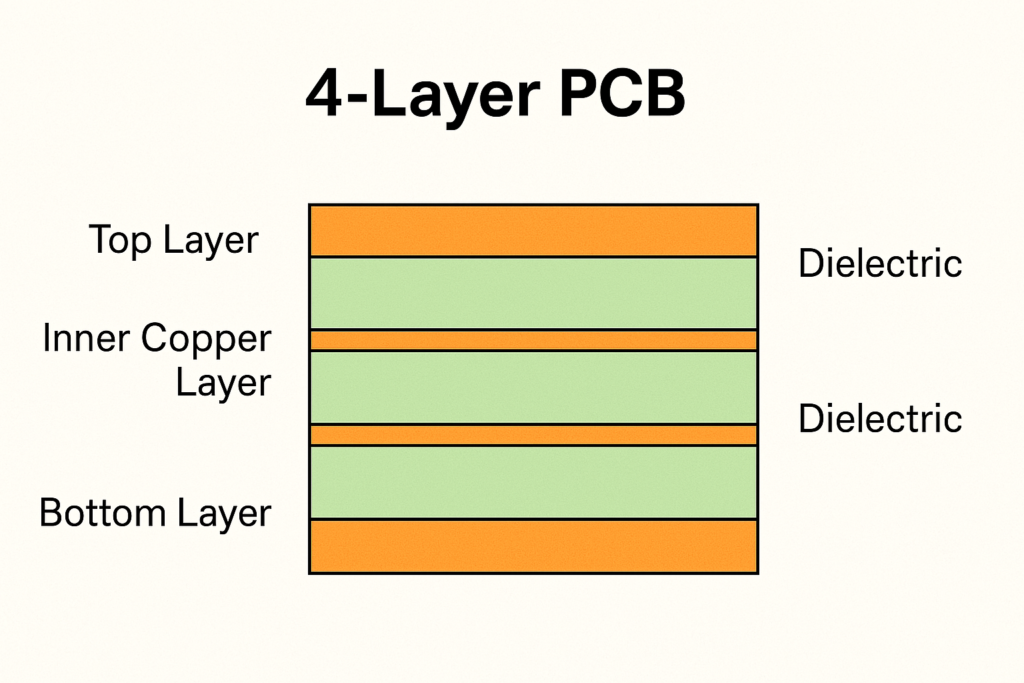
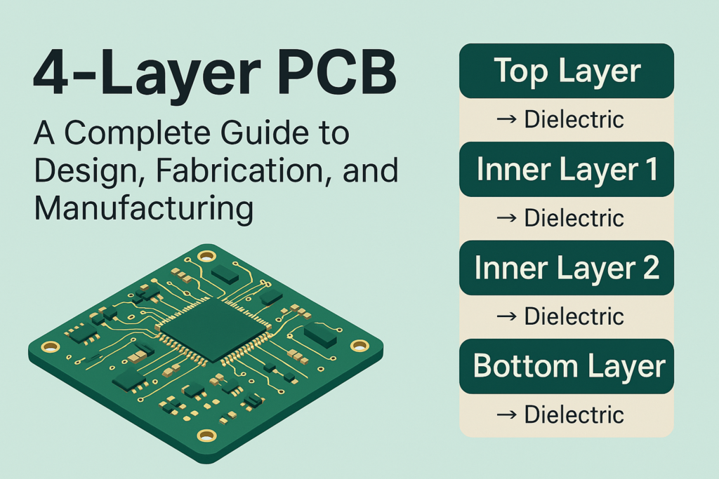
Structure and Functionality
- Layers:
- Top Layer (Layer 1): The surface layer where components are mounted, and traces are routed.
- Inner Layer 1 (Layer 2): Primarily used for power and ground planes, reducing electromagnetic interference and providing a stable reference for signals.
- Inner Layer 2 (Layer 3): Often used for signal routing or additional power and ground planes.
- Bottom Layer (Layer 4): Similar to the top layer, it can host components and carry traces.
- Advantages:
- Improved routing flexibility allows for more compact designs.
- Enhanced performance through better signal integrity and reduced noise due to dedicated ground and power planes.
- Increased thermal management capabilities.
- Reduced EMI and crosstalk
- More reliable for high-speed PCB design
- Applications: Commonly used in a variety of applications, including consumer electronics, automotive systems, telecommunications equipment, and industrial machines.
How to Make a 4-Layer PCB in Altium
Altium Designer is one of the most widely used EDA (Electronic Design Automation) tools for professional
PCB design Creating a 4-layer PCB in Altium Designer involves several steps, from schematic capture to PCB layout. Here’s a concise guide to get started.
Step-by-Step Process
- Define Your Project:
- Create a new PCB project in Altium Designer, and define the project parameters, including the layer stackup.
- Schematic Design:
- Generate a schematic by placing and interconnecting components using the schematic editor.
- Use Altium’s library to select standard components, or create custom ones as needed.
- Ensure all connections and electrical rules are validated.
- Define Layer Stack:
- Navigate to the Layer Stack Manager (Design > Layer Stack Manager).
- Set up your 4-layer configuration by adding two signal layers, a power layer, and a ground layer. Specify thicknesses and materials.
- PCB Layout:
- Switch to the PCB layout workspace and import your schematic.
- Place components onto the PCB and arrange them according to your design needs.
- Route signals, making sure to follow best practices for trace width and spacing.
- Design Rule Checks (DRC):
- Run design rule checks to find and rectify any layout issues, ensuring the circuit will function as intended.
- Generate the Gerber Files:
- Once the design is complete and errors resolved, generate the Gerber files needed for fabrication.
- Navigate to File > Fabrication Outputs > Gerber Files, and configure the output settings as required.
- Manufacturing:
- Choose a PCB fabrication service, upload your Gerber files, and specify any additional requirements such as surface finish and color of solder mask.
Altium’s simulation and 3D preview tools allow designers to visualize and validate the entire design before sending it for fabrication.
Are 4-Layer PCBs More Expensive?
The cost of PCBs depends on multiple factors, including layer count, manufacturing processes, materials used, and order volume. Generally, 4-layer PCBs tend to be more expensive than 2-layer boards due to several reasons:
Cost Factors
- Material and Process Costs:
A 4-layer PCB requires more materials and labor during the fabrication process. More copper and substrate material are needed, along with additional processing steps.
- Layer Complexity:
Each additional layer increases the complexity of the manufacturing process. The need for accurate alignment and layering contributes to higher costs.
- Volume Discounts:
Costs may be lower per unit for larger production runs due to economies of scale. However, for low-volume orders, 4-layer designs can be significantly pricier compared to simpler boards.
- Specification Requirements:
Higher-quality specifications (like tighter tolerances and higher frequency capabilities) often drive costs up.
However, the cost is justified in many cases because:
- They reduce the need for additional boards
- Allow tighter designs and smaller enclosures
- Improve signal and power integrity, reducing rework and EMI issues
Cost-saving tips:
- Optimize design for manufacturability
- Minimize board size
- Reduce the number of vias and layer transitions
- Use standard board sizes and finishes
4-Layer PCB Design
Designing a 4-layer PCB involves strategic planning to optimize space and performance while ensuring signal integrity and minimizing electromagnetic interference (EMI). Here are key design considerations:
Design Considerations
- Layer Stackup:
Determine the optimal stackup arrangement based on the intended application. Typical configurations include signal/power/ground/signal or signal/signal/ground/power designs.
- Trace Width and Spacing:
Calculate appropriate trace widths based on current-carrying requirements and manage spacing to prevent crosstalk and ensure compliance with design rules.
- Impedance Control:
For high-frequency applications, maintain consistent impedance by controlling trace dimensions and distances to reference planes.
- Ground Planes:
Use solid ground planes to reduce noise and provide a reference point for signals. Ensure proper grounding techniques to avoid ground loops.
- Thermal Management:
Consider heat dissipation paths for components that generate heat. Implement thermal vias or use thicker copper for power traces as necessary.
- Component Placement:
Plan component layout to minimize trace lengths, especially for high-frequency signals. Prioritize placement of critical components to enhance performance.
- 4. EMI/EMC Mitigation
- Short return paths
- Shield high-frequency signals with planes
- Use guard traces or copper pour for noisy areas
By following these design principles, engineers can create efficient and effective 4-layer PCB layouts that will perform reliably in their intended applications.
4-Layer PCB Example
To illustrate the application of a 4-layer PCB, consider a modern wireless communication module used in a smartphone. This module can serve as a prime example highlighting the key elements of 4-layer design.
Example: Wireless Communication Module
Breakdown of the Design:
- Top Layer:
Components such as RF amplifiers and antennas are mounted on the top layer. This layer contains traces for signal routing.
- Inner Layer 1:
Designed as a ground plane to minimize noise received by sensitive RF components and to provide a reliable reference for signal integrity.
- Inner Layer 2:
Used for routing high-frequency signals, including data communication links. It may also feature power distribution paths to critical components.
- Bottom Layer:
Contains additional components like decoupling capacitors and traces connecting to the power supply input. It is important for reducing overall height in compact designs.
Benefits of the 4-Layer Design:
- Reduced Noise: Having dedicated ground planes significantly lowers electromagnetic interference.
- Compact Size: Enabling a more compact layout allows greater integration of components, crucial for space-constrained designs like smartphones.
- Improved Performance: Optimized signal paths contribute to better performance rates for data transmission and reduced latency.
This example illustrates how 4-layer PCBs can meet the high demands of modern electronics while optimizing space and maintaining performance integrity.
4-Layer PCB Thickness
PCB thickness is an essential factor in design, affecting mechanical stability, thermal performance, and flexibility. For 4-layer PCBs, several thicknesses can be used, but common standards include:
Standard Thicknesses
- 1.6 mm (0.063 in): This is the most common thickness for PCBs and is used in many standard applications.
- 0.8 mm (0.031 in): Often used in thinner devices where space is at a premium.
- 1.0 mm (0.040 in): Suitable for applications that require a balance between rigidity and weight.
Typical thickness structure:
- Top Layer to Inner Layer 1: ~0.2 mm
- Core (between Inner Layers): ~0.8 mm
- Inner Layer 2 to Bottom Layer: ~0.2 mm
Factors Influencing Thickness
- Mechanical Strength: Thicker PCBs can withstand more mechanical stress, making them ideal for more robust applications.
- Thermal Management: The thickness affects thermal performance; a thicker board can dissipate heat more effectively, which is crucial for power-sensitive circuits.
- Flexibility Requirements: For applications requiring bending or flexing (like flexible PCBs), thinner PCBs are often chosen.
When designing a 4-layer PCB, understanding how thickness interacts with other design parameters is essential for ensuring the PCB meets all performance and mechanical requirements.
4-Layer PCB Stackup
The stackup configuration of a 4-layer PCB refers to how the layers are arranged and how they relate to each other in terms of signal and power routing. The effectiveness of a PCB stackup design dramatically impacts electrical performance and manufacturing processes.
Common Stackup Configurations
- Type 1 Stackup:
- Layer 1: Signal
- Layer 2: Ground Plane
- Layer 3: Power Plane
- Layer 4: Signal
This configuration is widely used when dedicated ground and power planes are necessary for maintaining signal integrity.
- Type 2 Stackup:
- Layer 1: Signal
- Layer 2: Signal
- Layer 3: Ground Plane
- Layer 4: Power Plane
This configuration provides enhanced routing for two signal layers while optimizing noise reduction through dedicated planes.
Design Considerations for Stackup
- Impedance Control: The dielectric thickness and the distance between signal and reference planes directly affect impedance and must be calculated accurately.
- Thermal Properties: The stackup will influence how heat flows through the PCB, impacting reliability and lifespan.
- Signal Integrity: Proper arrangements can reduce cross-talk and enhance signal quality, particularly vital for high-speed applications.
When designing 4-layer PCBs, careful consideration of the stackup can optimize the board for performance and manufacturability.
4-Layer PCB KiCad
KiCad is a free, open-source PCB design tool that enables engineers to create complex PCBs, including 4-layer boards. Creating a 4-layer PCB in KiCad may seem intimidating at first, but it follows a logical sequence.
Steps to Create a 4-Layer PCB in KiCad
- Installation: Ensure you have the latest version of KiCad installed on your computer.
- Project Setup: Start a new project and define project parameters. Open the PCB Editor and choose “File” > “New Board.”
- Define Layer Stack: Go to File > Board Setup, and under the “Layers” tab, configure the stackup to include four layers (two signals, one ground, one power).
- Schematic Capture: Open the Schematic Editor and design your circuit, placing components and creating connections.
- PCB Layout: Import the schematic into the PCB layout. Arrange components based on your design criteria and begin routing traces.
- Design Rule Checks (DRC): Use the DRC tool to validate your layout against the rules defined in the board setup. Fix any issues highlighted by the check.
- Export Gerber Files: Navigate to File > Plot to export the Gerber files for manufacturing. Make sure to configure settings to match your fabricator’s requirements.
- Manufacturing: Choose a PCB manufacturing service, submit the Gerber files, and specify any additional requirements like solder mask color or surface finish.
By following these steps, users can effectively leverage KiCad to design and manufacture their own 4-layer PCBs, making it accessible to hobbyists and professionals alike.
Conclusion
The 4-layer PCB bridges the gap between simple two-layer boards and complex multilayer designs. It provides a reliable platform for medium-to-complex circuits where signal integrity, power distribution, and EMI control are essential.
Whether you’re working with Altium, KiCad, or another EDA tool, understanding the principles of stackup, routing, and layer assignment is vital for effective PCB design. Furthermore, collaborating with experienced PCB fabrication and manufacturing partners can help reduce costs and ensure quality.
The next time your project needs compact routing, better EMC control, or faster signals, consider using a 4-layer PCB.