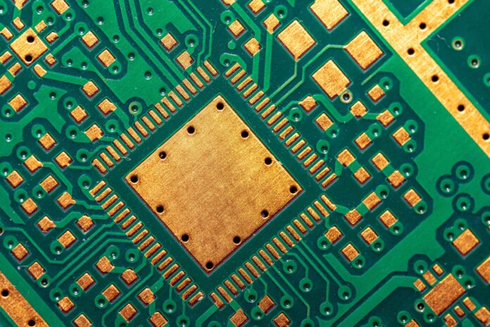
Designing printed circuit boards (PCBs) is a complex and meticulous task that requires a deep understanding of electronics, materials, and manufacturing processes. Even experienced engineers can fall into common traps that lead to costly errors, delays, and suboptimal performance. Identifying and avoiding these mistakes is crucial to producing reliable and efficient PCBs. Here are ten common mistakes in PCB design and how to avoid them.
In this blog post we will talk about:
- What are The Common Mistakes in PCB Design?
- 1. Inadequate Component Placement
- 2. Ignoring Thermal Management
- 3. Inadequate Power Distribution
- 4. Incorrect Trace Widths
- 5. Poor Signal Integrity
- 6. Inadequate Grounding
- 7. Insufficient Design for Manufacturability (DFM)
- 8. Overlooking Design for Test (DFT)
- 9. Not Considering Electromagnetic Compatibility (EMC)
- 10. Incomplete Documentation
- How Arshon Technology Can Help
What are The Common Mistakes in PCB Design?
1. Inadequate Component Placement
Poor component placement can lead to signal integrity issues, increased noise, and difficulties in assembly.
Solution:
Plan the layout by grouping related components together and placing them in a logical sequence. High-speed components should be placed as close to each other as possible to minimize trace lengths. Ensure adequate spacing for heat dissipation and accessibility for testing and maintenance.
2. Ignoring Thermal Management
Failing to account for heat dissipation can result in overheating, leading to reduced performance and potential damage to components.
Solution:
Use thermal vias, heat sinks, and copper pours to manage heat effectively. Place heat-generating components strategically and ensure there is sufficient airflow. Simulate thermal performance during the design phase to identify and mitigate potential issues.
3. Inadequate Power Distribution
Improper power distribution can cause voltage drops, noise, and instability in the circuit.
Solution:
Design a robust power distribution network with wide traces or power planes to minimize resistance and inductance. Use decoupling capacitors near power pins to filter out noise. Ensure that power and ground planes are continuous and have low impedance.
4. Incorrect Trace Widths
Using incorrect trace widths can lead to excessive resistance, voltage drops, and potential failure due to overheating.
Solution:
Calculate trace widths based on the current they will carry, considering factors such as temperature rise and allowable voltage drop. Use PCB design tools that include trace width calculators to ensure accuracy.
5. Poor Signal Integrity
Neglecting signal integrity can result in crosstalk, electromagnetic interference (EMI), and signal degradation.
Solution:
Keep high-speed signal traces short and direct, and route them over continuous ground planes. Use controlled impedance traces for high-frequency signals and differential pairs where necessary. Maintain proper spacing between traces to reduce crosstalk.
6. Inadequate Grounding
Poor grounding can lead to noise, interference, and unstable operation of the PCB.
Solution:
Implement a solid ground plane to provide a low-impedance path for return currents. Use multiple ground vias to connect different layers and ensure consistent grounding throughout the board. Avoid creating ground loops, which can introduce noise.
7. Insufficient Design for Manufacturability (DFM)
Ignoring DFM guidelines can lead to manufacturing defects, increased costs, and delays.
Solution:
Work closely with your manufacturer to understand their capabilities and limitations. Follow DFM guidelines for trace widths, spacing, hole sizes, and component placement. Use design rule checks (DRC) to identify and correct potential issues before production.
8. Overlooking Design for Test (DFT)
Neglecting DFT can make it difficult to test and debug the PCB, leading to increased troubleshooting time and costs.
Solution:
Incorporate test points for critical signals and power lines. Design the PCB to accommodate automated testing equipment and ensure accessibility for probes and connectors. Implement boundary scan techniques for complex designs.
9. Not Considering Electromagnetic Compatibility (EMC)
Failing to address EMC can lead to interference with other electronic devices and failure to meet regulatory standards.
Solution:
Design with EMC in mind by using proper shielding, filtering, and grounding techniques. Avoid long parallel traces and minimize loop areas to reduce radiated emissions. Simulate EMC performance and conduct pre-compliance testing to identify and mitigate issues early.
10. Incomplete Documentation
Inadequate documentation can result in misunderstandings, errors in manufacturing, and difficulties in troubleshooting.
Solution:
Provide comprehensive documentation, including schematics, layout files, bill of materials (BOM), and assembly drawings. Clearly annotate critical information, such as component values, test points, and special instructions. Ensure that all stakeholders have access to the latest version of the documentation.
How Arshon Technology Can Help
Arshon Technology has extensive experience in PCB design, helping clients avoid these common pitfalls. Our team of experts ensures that every aspect of your PCB design is meticulously planned and executed, from initial concept to final production.
Component Placement and Layout
We use advanced design tools and methodologies to optimize component placement and layout for performance, reliability, and manufacturability.
Thermal Management
Our designs incorporate effective thermal management solutions to ensure your PCBs operate within safe temperature ranges.
Power and Signal Integrity
We design robust power distribution networks and signal integrity solutions to prevent noise and ensure stable operation.
Manufacturing and Test Considerations
Our designs follow industry best practices for DFM and DFT, reducing the risk of manufacturing defects and simplifying testing and debugging.
EMC Compliance
We address EMC issues during the design phase to ensure your PCBs meet regulatory standards and perform reliably in real-world environments.
Comprehensive Documentation
We provide detailed documentation to support manufacturing, assembly, and troubleshooting, ensuring a smooth transition from design to production.
By leveraging Arshon Technology’s expertise, you can avoid common PCB design mistakes and achieve high-quality, reliable, and cost-effective PCBs. Contact us today to learn more about how we can support your PCB design projects.
