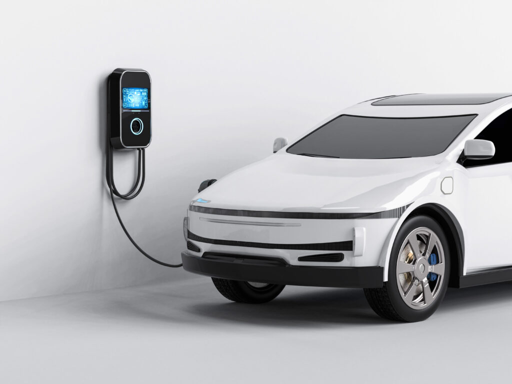
: A Game-Changer for Electric Vehicle Charging")
The rise of electric vehicles (EVs) has revolutionized the automotive industry, and with it, the demand for efficient and versatile charging solutions has increased significantly. One of the most prominent advancements in this area is the Combined Charging System (CCS). Designed to offer both fast and reliable charging, the CCS is now a global standard for EV manufacturers. It combines both AC (Alternating Current) and DC (Direct Current) charging capabilities into a single connector, providing flexibility for EV users, whether they are at home or using public charging stations.
This blog delves into how CCS operates, the role of electronic design and PCB design in its development, and how this technology is shaping the future of EV infrastructure.
What is the Combined Charging System (CCS)?
The Combined Charging System is a unified charging protocol developed to standardize EV charging across the globe. Unlike older systems that required separate connectors for AC and DC charging, CCS simplifies this process by combining both into a single connector, streamlining the charging experience.
AC Charging:
AC charging, typically slower, is suitable for overnight home charging or long-term parking. It is ideal when speed is not a priority but convenience is.
DC Fast Charging:
DC charging is much faster and is used in public fast-charging stations. It bypasses the vehicle’s onboard charger and directly supplies the battery with high power, allowing EV drivers to recharge quickly, often in under an hour.
The versatility of CCS has made it the preferred standard among EV manufacturers in Europe, North America, and beyond. Its growing adoption is further accelerating the infrastructure necessary for the mass adoption of EVs worldwide.
How CCS Works
The CCS connector uses a combination of both AC and DC pins. When charging at home or using a slower public charger, the AC pins are utilized. On the other hand, the DC pins come into play when connecting to a high-power fast charger. This hybrid design not only simplifies charging but also reduces the complexity and cost of integrating multiple charging interfaces into an EV.
This system also communicates with the vehicle’s battery management system (BMS) to ensure that the right amount of current and voltage is supplied to the battery, optimizing charging time and maintaining safety.
The Role of Electronic Design in CCS Development
The success of the Combined Charging System hinges heavily on sophisticated electronic design. Ensuring that the charging process is efficient, safe, and capable of handling high power transfers requires careful attention to the power electronics embedded within the charging system.
Power Conversion Efficiency:
One of the most critical challenges in electronic design for CCS is ensuring high power conversion efficiency. EV charging involves transforming the alternating current (AC) from the grid into the direct current (DC) required by the vehicle’s battery. Power electronics such as rectifiers, converters, and inverters must be carefully designed to minimize energy losses during this conversion process, as inefficiencies can lead to longer charging times and increased energy costs.
Voltage Regulation:
During DC fast charging, large amounts of power are transferred to the battery in a very short time. To avoid overloading the battery and ensure a stable energy transfer, the system’s electronic design must include precise voltage regulation circuits. These regulate the incoming power and adjust the voltage levels as needed, preventing overheating and protecting the battery from potential damage.
Safety Features:
Safety is paramount in any EV charging system, particularly with the higher power levels involved in fast charging. Designers must incorporate protective measures such as overcurrent protection, surge protection, and temperature monitoring to prevent electrical failures and hazards during charging. Ensuring safe operation under both AC and DC modes is a complex task that relies on cutting-edge electronic design strategies.
The challenges extend beyond the vehicle itself. The charging station, including its connectors, also requires advanced electronic design to handle varying current and voltage levels while maintaining communication with the vehicle. This two-way communication ensures the charging process is adaptive and secure.
PCB Design and Its Critical Role in CCS
The intricate electronics behind CCS charging rely heavily on the physical layout of their internal circuitry. This is where PCB design plays a pivotal role. The printed circuit board (PCB) is the backbone of any electronic system, facilitating electrical connections and signal transmission between various components.
High-Power Applications:
CCS charging stations, particularly those capable of DC fast charging, must handle high current loads and voltages. Designing PCBs for such high-power applications is no easy task. The copper traces on the PCB must be sufficiently thick to handle the current without overheating, and the layout must be optimized to minimize electrical resistance and power losses.
In a fast-charging scenario, energy transfer rates can be as high as 350 kW, which puts immense strain on the PCB components. Designers must carefully balance the layout to ensure the board can safely handle this power without generating excessive heat.
Thermal Management:
Heat dissipation is another key concern in PCB design for CCS. High current loads generate heat, which can degrade components over time if not managed properly. Therefore, designers often incorporate thermal vias, heat sinks, and specialized thermal management materials into their PCBs. These components help spread the heat more evenly across the board and keep critical areas from overheating.
Electromagnetic Interference (EMI):
The complex electronics involved in CCS are susceptible to electromagnetic interference (EMI), which can affect the performance of the charging system and even disrupt communication between the vehicle and the charging station. To mitigate these risks, PCB designers employ advanced layout techniques such as proper trace routing, grounding, and shielding. Minimizing EMI is crucial for ensuring reliable operation in high-power environments.
Multi-Layer PCB Design:
Given the complexity of CCS charging stations, multi-layer PCB designs are often required. A multi-layer PCB allows designers to fit more components into a smaller area by stacking multiple layers of circuitry on top of each other. This is especially important for fast chargers, which must include sophisticated power electronics, communication circuits, and safety features, all within a compact enclosure.
Signal Integrity:
Another critical aspect of PCB design for CCS is maintaining signal integrity. The communication between the charging station and the vehicle is essential for coordinating the charging process. Any loss or corruption of these signals can lead to charging interruptions or, in worst cases, damage to the vehicle’s battery. Signal integrity issues often arise from poor PCB layout or inadequate shielding, making careful design essential for reliable performance.
The Future of CCS and Its Impact on Electronic and PCB Design
As the EV market continues to grow, the demand for more advanced and efficient charging technologies will push the boundaries of electronic design and PCB design even further. The next generation of CCS systems is likely to support even higher power levels, reducing charging times to just a few minutes. This will require innovations in heat management, power efficiency, and safety features, placing new demands on both the electronic components and the PCBs they rely on.
Furthermore, emerging technologies such as wireless charging and vehicle-to-grid (V2G) integration are likely to be incorporated into future CCS systems. These advancements will add new layers of complexity to the design process, requiring PCBs and electronic systems that can handle wireless power transfer while ensuring that communication and control signals remain stable and secure.
Conclusion
The Combined Charging System (CCS) represents a significant leap forward in the EV charging landscape, offering the flexibility of both AC and DC charging in a single interface. Behind this innovation lies a wealth of engineering expertise, particularly in the realms of electronic design and PCB design.
As electric vehicles continue to proliferate, the demand for fast, efficient, and safe charging solutions will only grow. Innovations in electronic design will enable faster charging times and better energy management, while advancements in PCB design will ensure that these systems remain compact, reliable, and safe for users. As CCS evolves, it will play a crucial role in shaping the future of EV infrastructure, making it easier for drivers to charge their vehicles and pushing the boundaries of what’s possible in the world of electronic and PCB design.