
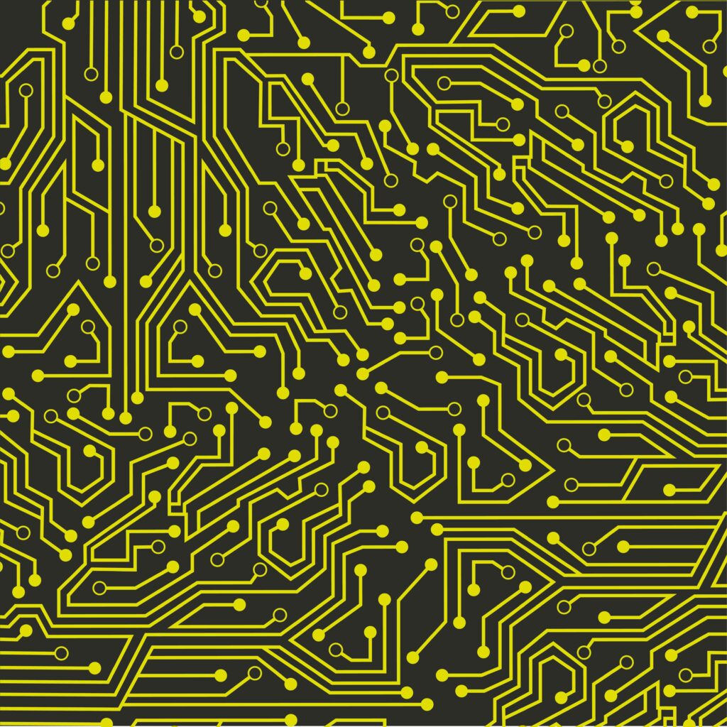
PCB etching is essential in PCB design, transforming a copper-clad board into a functional printed circuit through copper removal. This subtractive process leaves behind the precise pathways needed to connect electronic components, allowing accurate circuit formation. In this article, we’ll explore the different etching methods, materials involved, quality control practices, and technological advancements that enhance efficiency and environmental responsibility, supporting both simple and complex circuit designs across various industries.
Introduction to PCB Etching
PCB etching is fundamental to circuit design, where unnecessary copper is removed to create specific electrical paths. The process starts with a copper-coated substrate, which undergoes etching to retain only the required conductive traces. This approach is vital for applications from simple single-layer boards to complex multilayer systems.
PCB Etching Methods
PCB etching methods are generally divided into wet etching and dry etching techniques, each suitable for different circuit requirements:
Wet Etching:
The most common technique, wet etching, uses chemical solutions such as ferric chloride or ammonium persulfate to dissolve unprotected copper. This method is cost-effective and fast, ideal for high-production volumes. However, it requires careful chemical handling and waste disposal.
Dry Etching:
Dry etching utilizes plasma or laser technology to remove copper without chemicals. It is more precise than wet etching, allowing for extremely fine traces suitable for high-frequency applications. Dry etching is more costly but provides accuracy that meets the demands of advanced electronics.
Materials in PCB Etching
Several materials play a role in the etching process:
- Copper-Clad Laminate: The base material is typically a fiberglass or epoxy layer coated in copper.
- Photoresist: This light-sensitive material is applied to the copper surface and hardened over areas to be retained, serving as a protective layer during etching.
- Etching Solution: Solutions like ferric chloride and sodium persulfate dissolve exposed copper, revealing the final circuit design.
PCB Etching Process Steps
The PCB etching process involves several key steps to achieve precise results:
Design Transfer:
Using design software, the layout is created and transferred to the board using a photomask or direct print.
Photoresist Application:
The photoresist layer is applied to the copper surface.
Exposure and Development:
The board is exposed to UV light through the design mask, hardening the photoresist on areas that should remain copper-covered.
Etching:
The board is submerged in an etching solution, which dissolves unprotected copper.
Photoresist Removal:
After etching, the remaining photoresist is removed, leaving the intended copper traces.
Quality Control in PCB Etching
Quality control is vital to ensure that PCB etching meets design standards. Key inspection methods include:
- Microscopy: Examining under-etched or over-etched areas and confirming trace accuracy.
- Electrical Testing: Testing for continuity, ensuring there are no breaks or shorts in the circuit.
- Optical Inspection: Automated Optical Inspection (AOI) detects any design flaws, verifying adherence to specifications.
Thorough quality control minimizes issues like incomplete circuits and prevents short circuits.
Environmental and Safety Considerations
Chemical etching, particularly with ferric chloride, creates hazardous waste. Proper disposal and recycling practices are essential to reduce environmental impact. Many manufacturers reclaim copper from waste etchants to support sustainability. Dry etching produces less chemical waste but requires proper ventilation and protective measures for operators.
Advances in PCB Etching Technology
Recent innovations in PCB etching have enhanced precision and environmental responsibility:
- Laser Etching: Laser etching is increasingly popular for applications requiring fine trace widths, such as microelectronics and wearables.
- Automated Etching Machines: Automation allows for consistent, controlled etching processes, increasing accuracy and speed.
- Eco-Friendly Solutions: Environmentally safe etchants are being introduced to reduce the use of hazardous chemicals.
Choosing the Right Etching Technique
Selecting an etching technique depends on factors like board complexity, trace width, production volume, and environmental impact. Wet etching is suitable for standard boards and high production volumes due to its cost-effectiveness, while dry etching is preferred for designs requiring narrow traces. The choice of etching method can also depend on factors such as the substrate material and layer count.
Conclusion
PCB etching is a foundational process in creating precise and reliable circuits. Through either wet or dry methods, PCB etching helps transform copper-clad boards into the intricate designs necessary for various applications. By understanding the etching process, materials, and quality control measures, manufacturers can achieve efficient, high-quality results suited to diverse industry needs.