
Printed Circuit Boards (PCBs) are integral to modern electronic devices, driving innovation by serving as the foundation for circuit connectivity. As technology advances, the demand for compact, high-performing devices has skyrocketed, placing PCB designers under constant pressure to optimize space without compromising functionality. One of the key advancements in PCB technology that addresses this challenge is the use of blind vias.
Blind vias play a significant role in reducing PCB size and improving its overall performance. This article explores the concept of blind vias, their functionality, benefits, and the role they play in modern PCB design.
What Are Blind Vias?
Blind vias are specialized holes or pathways in a PCB that connect the surface layer of the board to one or more inner layers without passing all the way through the board. Unlike through-hole vias, which extend through the entire thickness of the PCB, blind vias terminate at a designated inner layer.
These vias are created using advanced drilling or laser techniques, allowing designers to precisely control their depth and location. By limiting the depth of the via, PCB manufacturers can optimize space usage and reduce signal interference.
How Are Blind Vias Fabricated?
The fabrication of blind vias involves a series of precise steps to ensure their accuracy and reliability. The most common methods include:
- Laser Drilling:
- A laser is used to create micro-sized blind vias with high precision.
- Suitable for high-density interconnect (HDI) PCBs.
- Mechanical Drilling:
- A mechanical drill bores the blind via to the desired depth.
- More cost-effective but less precise compared to laser drilling.
- Sequential Lamination:
- Layers of the PCB are laminated together with blind vias drilled into specific layers before the final assembly.
Each method is chosen based on the design complexity, budget, and application requirements.
The Role of Blind Vias in PCB Design
1. Space Optimization
Blind vias are a game-changer in reducing the overall size of a PCB. By connecting only the required layers, they free up space on other layers for additional components or routing. This capability is crucial in compact devices like smartphones, wearable technology, and medical implants where every millimeter counts.
2. Improved Signal Integrity
In high-speed circuits, signal integrity is a major concern. Blind vias help by reducing the length of signal pathways, minimizing signal distortion, and preventing cross-talk between layers. This results in better performance, especially in HDI PCBs.
3. Enhanced Design Flexibility
Blind vias offer greater flexibility in layer stacking and routing, enabling designers to create more complex multilayer PCBs. This flexibility is essential for developing cutting-edge technologies that require intricate circuit layouts.
4. Cost Efficiency in Advanced Designs
While blind vias can initially increase manufacturing costs due to specialized processes, they often lead to overall cost savings. By reducing PCB size, manufacturers save on material costs, and the end devices can be made smaller and lighter, which appeals to consumers.
Applications of Blind Vias
1. Consumer Electronics
The demand for compact and lightweight devices such as smartphones, tablets, and laptops has driven the widespread adoption of blind vias. These devices rely on HDI PCBs, where blind vias are a staple for dense component layouts.
2. Automotive Electronics
Modern vehicles are equipped with advanced driver-assistance systems (ADAS), infotainment systems, and sensors. Blind vias help integrate these technologies into the limited space available within automotive systems.
3. Medical Devices
Miniaturized medical devices, such as pacemakers and diagnostic equipment, benefit from blind vias by combining compactness with high performance.
4. Aerospace and Defense
In aerospace and defense applications, where space and weight are critical, blind vias allow for the integration of advanced functionalities without increasing the size of the equipment.
Challenges in Using Blind Vias
Despite their advantages, blind vias come with challenges that designers and manufacturers must address:
- Higher Fabrication Costs:
- Specialized drilling techniques and additional manufacturing steps can increase costs.
- Design Complexity:
- Incorporating blind vias requires advanced design software and expertise, making the design process more intricate.
- Thermal Management:
- Blind vias can create localized heat buildup if not designed properly, especially in high-power applications.
- Reliability Concerns:
- Poorly fabricated blind vias can lead to delamination or electrical failures, particularly in harsh environments.
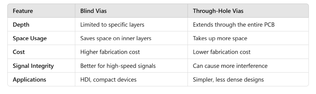
Blind Vias vs. Through-Hole Vias
To fully understand the benefits of blind vias, it is essential to compare them with through-hole vias:
Future Trends in Blind Vias
The growing demand for smaller, more powerful devices continues to drive innovation in PCB manufacturing. The role of blind vias will expand as technologies like:
1. 5G and Beyond:
- High-frequency circuits for 5G networks require precise and compact PCB designs, where blind vias are indispensable.
2. Internet of Things (IoT):
- IoT devices often prioritize size and efficiency, relying heavily on HDI PCBs with blind vias.
3. Wearable Technology:
- Blind vias will play a crucial role in integrating complex circuits into compact, wearable devices.
4. Advanced Manufacturing Techniques:
- The development of more cost-effective and reliable fabrication methods for blind vias will make them accessible for a broader range of applications.
Conclusion
Blind vias have revolutionized PCB design by enabling compact, high-performance circuits in a variety of industries. Their ability to optimize space, improve signal integrity, and enhance design flexibility makes them an invaluable tool for modern electronics. While they come with challenges such as higher costs and design complexity, advancements in manufacturing techniques and growing demand for miniaturization are driving their adoption.
As technology continues to evolve, the role of blind vias in reducing PCB size and enabling innovative applications will only grow, cementing their place as a cornerstone of advanced PCB design. Whether in consumer electronics, automotive systems, or medical devices, blind vias are a key enabler of the small, powerful devices that define our modern world.