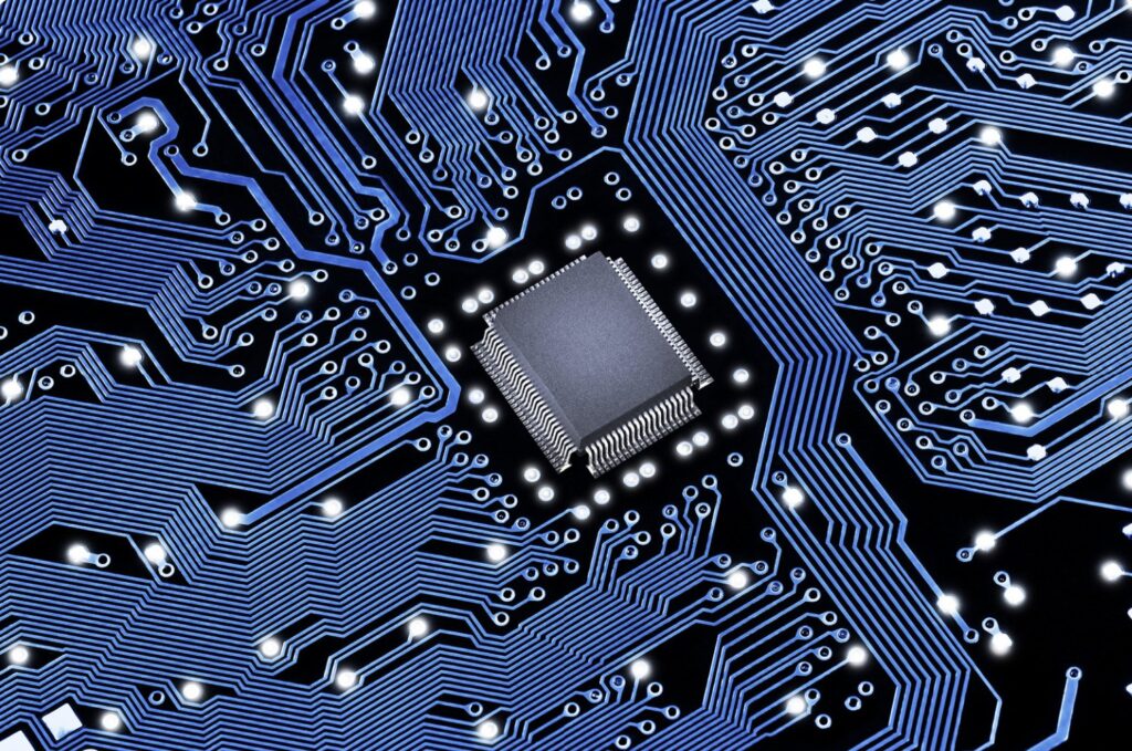
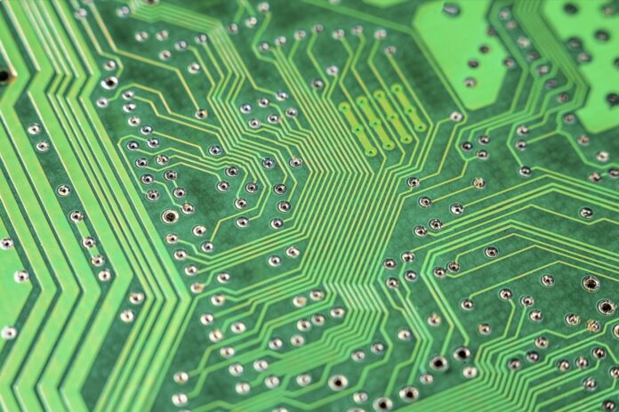
Microvia technology is essential in modern PCB design, supporting the shift toward smaller, high-density devices packed with advanced features. In essence, a microvia is a small hole in a printed circuit board (PCB) that connects different layers electrically. Microvias are essential in high-density interconnect (HDI) PCBs, which are designed to achieve high routing density, better signal integrity, and advanced functionality in minimal space. With the growing demands in industries like telecommunications, aerospace, automotive, and consumer electronics, microvia technology has enabled the production of high-performance PCBs for advanced applications.
Understanding Microvia Technology
A microvia is defined by the IPC (Institute of Printed Circuits) as a via with a diameter of 150 microns or less, typically drilled by laser. Unlike traditional through-hole vias, which go through the entire PCB, microvias are often “blind” or “buried” vias, connecting only specific layers without penetrating the entire board. This makes them ideal for HDI PCBs, as they allow more layers and components to fit within a smaller footprint.
The use of microvias has expanded as devices have become more complex and compact. Microvias enable PCBs to have fine-pitch components, which are common in mobile devices and high-frequency applications. Microvia technology can be implemented in multiple configurations, including blind, buried, stacked, and staggered microvias, each with specific uses based on design requirements.
Types of Microvias
Microvias come in several configurations depending on the requirements of the PCB:
Blind Microvias:
These connect an outer layer to one or more inner layers without passing through the entire board. They are commonly used in HDI designs for direct connections between surface components and inner layers.
Buried Microvias:
These vias connect two or more internal layers without reaching the outer layers. Buried microvias are useful in complex designs where internal layer interconnections are necessary without affecting surface components.
Stacked Microvias:
Multiple microvias are stacked on top of each other to connect multiple layers, providing increased interconnect density. Stacked microvias require precise alignment and are often more costly due to additional processing requirements.
Staggered Microvias:
These microvias are offset, connecting layers without directly overlapping each other. Staggered microvias provide flexibility in routing without the alignment challenges of stacked microvias.
Each of these microvia types serves specific design purposes, allowing engineers to choose the optimal configuration based on space, cost, and signal integrity requirements.
Benefits of Microvia Technology
Microvia technology offers several key advantages over traditional through-hole vias, particularly for applications requiring high-density interconnections and compact design. Some of the major benefits include:
- Enhanced Signal Integrity: Microvias reduce parasitic inductance and capacitance compared to larger vias, leading to better signal integrity. This is crucial in high-frequency applications where interference and signal loss can affect performance.
- Space Efficiency: Microvias allow for more routing density within the same PCB area, enabling designers to pack more functionality into smaller devices. This is especially important in consumer electronics, where compact size is a priority.
- Improved Thermal Management: The smaller size of microvias facilitates better heat dissipation in densely populated PCBs, which is vital in applications with high power requirements.
- Layer Reduction: Since microvias can connect specific layers directly without traversing the entire PCB, designers can often reduce the number of layers required for routing, leading to cost and weight savings.
- Increased Reliability: Microvias, especially when used in HDI PCBs, have been shown to improve board reliability due to their smaller size and minimized stress on interconnections.
Applications of Microvia Technology in Advanced Industries
The versatility and advantages of microvia technology make it suitable for a variety of industries with demanding performance requirements:
Telecommunications:
As the telecom industry adopts 5G technology, microvia-enabled HDI PCBs play a central role in creating high-speed, low-latency network infrastructure. Microvias are used in base stations, routers, and other telecom equipment to enable fast data processing and signal integrity at high frequencies.
Automotive:
In automotive applications, particularly in electric vehicles (EVs) and advanced driver-assistance systems (ADAS), microvia technology is used in power modules, sensors, and controllers. The ability to support high-density designs and thermal management makes microvias critical in the compact and power-sensitive automotive environment.
Aerospace and Defense:
The aerospace industry demands high reliability and durability in compact forms. Microvia technology allows for the production of lightweight, highly reliable PCBs for avionics, radar, and communications systems, meeting strict industry standards.
Consumer Electronics:
From smartphones and tablets to wearables and IoT devices, microvia technology enables compact, multi-functional designs. HDI PCBs with microvias are essential in achieving the small form factors and high performance required in modern consumer devices.
Medical Devices:
Medical devices require miniaturized components and reliable performance. Microvia technology is used in imaging equipment, diagnostic tools, and portable monitoring devices to support compact and intricate circuitry.

Challenges in Microvia Technology
Despite its advantages, implementing microvia technology involves several challenges:
- Manufacturing Complexity: Microvias require precision laser drilling and advanced materials, which increases manufacturing complexity. Tight tolerances are necessary to ensure alignment, especially for stacked microvias.
- Higher Costs: Compared to traditional vias, microvias can be more expensive due to the specialized processes and equipment required. However, the cost can be offset by the performance benefits and the reduction in layer count in many designs.
- Reliability Concerns: Microvias can suffer from thermal and mechanical stress, especially in high-temperature applications. Techniques such as copper filling and resin reinforcement are often used to enhance their durability.
- Material Compatibility: High-density designs using microvias often require materials with low coefficients of thermal expansion (CTE) to prevent cracking. Not all materials used in standard PCB manufacturing are suitable for microvia technology, making material selection critical.
- Testing and Quality Assurance: Testing microvias for structural integrity and alignment can be challenging due to their small size. Advanced inspection methods, like X-ray and laser-based testing, are often required to ensure quality.
Recent Advancements in Microvia Technology
The PCB industry has seen several innovations in microvia technology, aimed at improving performance, cost-effectiveness, and manufacturability:
- Laser-Drilled Microvias: Laser drilling has become the standard for creating microvias, offering precise control over via size and placement. The latest laser technology enables faster and more accurate drilling, allowing for higher yields and consistent results.
- Copper-Filled Microvias: Filling microvias with copper instead of leaving them as open holes enhances electrical performance and mechanical strength. Copper-filled microvias provide a more robust structure, allowing for better heat dissipation and current-carrying capacity.
- Embedded Component Technology (ECT): Embedding passive or active components within the PCB using microvias can further reduce size and enhance performance. This technology is especially beneficial in high-frequency applications and power electronics.
- Advanced Inspection Techniques: Automated Optical Inspection (AOI) and X-ray inspection are increasingly used to verify the quality of microvias. These techniques enable manufacturers to detect issues like misalignment, voids, and cracks, ensuring the reliability of high-density PCBs.
- Environmentally Friendly Processes: New manufacturing processes aim to reduce the environmental impact of microvia production. Techniques like using water-based cleaning agents and recycling copper waste align with the industry’s push toward sustainability.
Future of Microvia Technology
As electronic devices continue to evolve, microvia technology will play a key role in enabling higher density, increased functionality, and improved performance. With ongoing advancements in laser drilling, material science, and manufacturing processes, the reliability and cost-effectiveness of microvia technology are expected to improve further. The integration of microvias into flexible PCBs and multi-functional substrates, like those used in wearable technology and IoT devices, will open new possibilities for innovation across various fields.
Conclusion
Microvia technology is at the heart of high-density PCB design, allowing engineers to develop compact and powerful circuits for advanced applications. Through innovations in microvia configurations, materials, and manufacturing techniques, microvia technology continues to meet the increasing demands of industries ranging from telecommunications and automotive to consumer electronics and aerospace. As this technology evolves, it will remain a cornerstone in the development of high-performance, miniaturized electronics, enabling new breakthroughs in design and functionality.
