
Design technology has rapidly evolved over the decades, giving rise to specialized tools that cater to specific needs. Among the most notable are Electronic Design Automation (EDA) and Computer-Aided Design (CAD). While they share some similarities, these tools serve distinct purposes in engineering and design. This article unpacks the basics of EDA and CAD, exploring their differences, applications, and roles in shaping modern industries.
What is CAD?
Computer-Aided Design, or CAD, refers to the use of software to create, modify, analyze, or optimize designs. It’s a cornerstone of industries such as architecture, mechanical engineering, and manufacturing. CAD tools help designers visualize objects in 2D or 3D, enabling precise planning and adjustments before production.
Key Features of CAD:
- 3D Modeling: Tools like SolidWorks and AutoCAD allow for the creation of detailed three-dimensional models.
- Simulation and Analysis: CAD software often includes features to simulate stress, heat transfer, and other physical properties.
- Drafting: CAD replaces manual drafting with accurate and scalable digital drawings.
- Customization: Designers can create reusable templates and libraries to streamline workflows.
Industries Using CAD:
- Architecture: For building blueprints and structural designs.
- Automotive: Designing car components and assemblies.
- Aerospace: Creating detailed aircraft schematics.
- Product Design: Prototyping consumer products and packaging.
What is EDA?
Electronic Design Automation (EDA) is software specifically designed for the development of electronic systems. It’s indispensable in industries like semiconductor manufacturing and printed circuit board (PCB) design. Unlike CAD, which focuses on physical structures, EDA delves into the intricacies of electronic components and circuits.
Key Features of EDA:
- Schematic Capture: Tools for designing circuit schematics.
- Simulation: Predicting circuit behavior under various conditions.
- Layout Design: Creating PCB layouts with precision.
- Verification: Ensuring designs meet performance and reliability criteria.
Industries Using EDA:
- Semiconductors: Designing integrated circuits (ICs) and microprocessors.
- Consumer Electronics: Developing PCBs for devices like smartphones and laptops.
- Automotive: Electronics for modern vehicles, including sensors and control units.
- Telecommunications: Designing hardware for networking and communication systems.
Key Differences Between EDA and CAD
| Feature | EDA | CAD |
|---|---|---|
| Focus | Electronic systems and circuits | Mechanical and structural designs |
| Tools | SPICE, KiCad, Cadence Allegro | AutoCAD, SolidWorks, CATIA |
| Simulation | Circuit behavior | Physical properties (e.g., stress) |
| Applications | PCB, IC, and system design | Buildings, machines, and products |
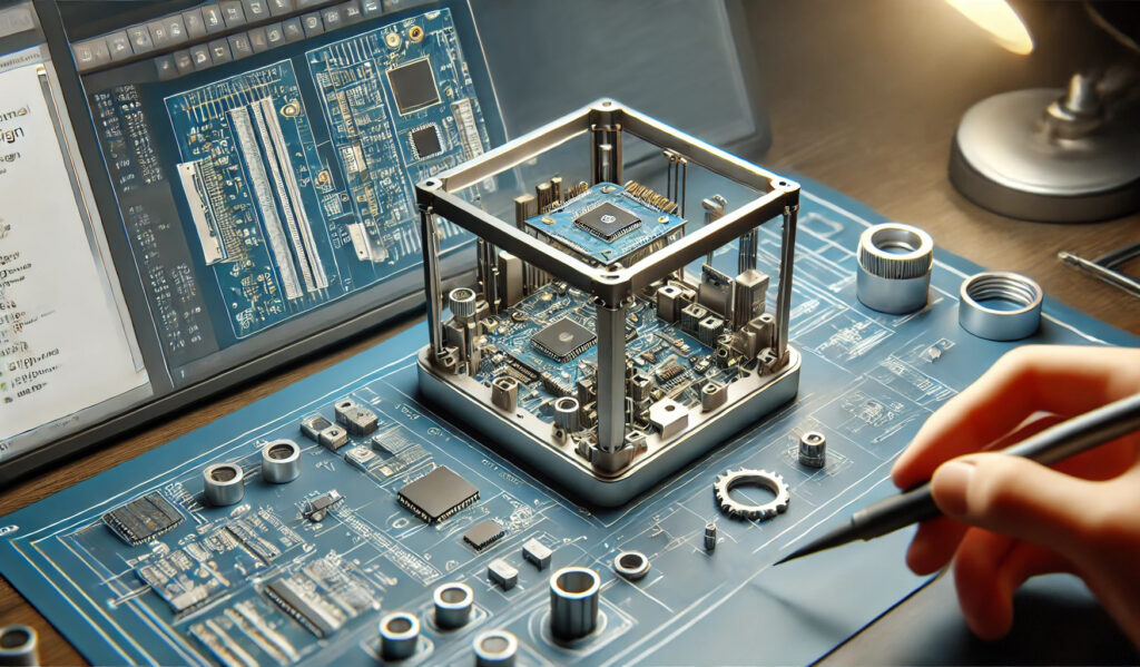
Integration Between EDA and CAD
While EDA and CAD cater to different domains, their integration is becoming increasingly important. For example, in IoT devices, the electronic components designed using EDA must fit within enclosures created in CAD. Software solutions are emerging to bridge this gap, allowing seamless collaboration between mechanical and electronic design teams.
The Future of Design Technology
The boundaries between EDA and CAD are blurring with advancements in technology. Tools now incorporate artificial intelligence (AI) and machine learning (ML) to optimize designs. Cloud-based solutions are enabling real-time collaboration across geographies. Moreover, industries like autonomous vehicles and smart cities are driving the need for integrated design approaches.
Conclusion
EDA and CAD are indispensable in their respective domains, but understanding their differences is crucial for leveraging their capabilities effectively. As technology evolves, these tools will continue to shape the future of engineering and design. Whether you’re an engineer, designer, or tech enthusiast, staying updated on these tools can provide a competitive edge in a rapidly changing landscape.