
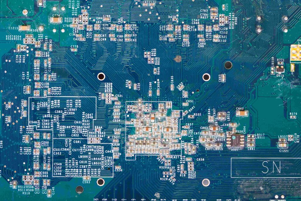
In the ever-evolving world of PCB Design and PCB Manufacturing, one often overlooked yet crucial factor is PCB surface roughness. As the demand for high-frequency, high-speed electronic products grows, the impact of PCB surface texture on signal integrity, impedance, and overall performance has become a primary concern for design engineers and manufacturing professionals alike.
PCB surface roughness refers to the microscopic texture of the PCB’s copper or dielectric surface. Even though these variations are measured in microns or nanometers, they can have a massive effect on signal loss, particularly in high-speed digital and RF/microwave circuits. This article will explore what PCB surface roughness is, how it is measured, its effect on PCB Design and PCB Manufacturing, and how to calculate and control it.
What is the Typical Surface Roughness of a PCB?
In PCB Manufacturing, surface roughness is a measure of the texture of the copper surfaces or dielectric materials. It quantifies the deviations in the surface profile, typically expressed in micrometers (μm) or microinches (μin).
Typical Copper Surface Roughness:
- Electrodeposited (ED) Copper Foil: 3 μm to 10 μm Ra (Roughness Average)
- Rolled Annealed (RA) Copper Foil: 0.5 μm to 2 μm Ra
- Very Low Profile (VLP) Copper Foil: 1 μm to 2 μm Ra
- Reverse Treated Foils: 1 μm to 3 μm Ra
Standard PCB Manufacturing processes generally result in a copper roughness of around 3 μm Ra. For applications requiring high signal integrity, smoother copper is often selected, such as VLP or RA copper, to reduce insertion loss and enhance performance in high-speed PCB Design.
What is the Ideal Surface Roughness?
The ideal surface roughness for a PCB Design depends on the intended application. In general:
- High-Speed Digital Circuits and RF Designs: Aim for copper roughness below 2 μm Ra.
- Standard Multilayer PCBs for General Applications: A copper roughness of 3 μm to 5 μm Ra is typically acceptable.
Why? Because smoother surfaces offer:
- Lower Conductor Loss: High-frequency signals travel near the surface of the conductor (skin effect). Increased surface roughness increases effective resistance, leading to higher insertion loss.
- Better Impedance Control: Smooth surfaces ensure consistency in trace dimensions, critical for maintaining characteristic impedance.
- Improved Laminate Bonding: However, while smoother surfaces reduce loss, very smooth copper may have poorer adhesion to dielectric substrates. Reverse treated copper or special bonding treatments often solve this problem.
Thus, PCB Manufacturers must balance electrical performance with mechanical adhesion when choosing surface roughness.
What are the 16 Rules for Surface Roughness?
The 16 Rules for Surface Roughness come from general manufacturing and machining guidelines. Although these are traditionally applied in metal machining, they can be adapted to PCB Manufacturing processes to understand PCB Surface Roughness control.
The 16 Rules (Adapted for PCB Context)
- Specify the Ra (Roughness Average) according to design needs.
- The smoother the surface, the higher the manufacturing cost.
- Tighter control requires stricter process monitoring.
- Higher surface roughness increases electrical resistance at high frequencies.
- Smoother copper increases the risk of delamination if bonding isn’t optimized.
- Adhesion promoters can mitigate bonding issues on smooth copper.
- Reverse treated foils balance roughness and adhesion.
- Surface roughness impacts dielectric loss and impedance.
- Consistency across panels is critical for repeatable PCB performance.
- Ra and Rz (maximum height) values should be specified clearly in design documents.
- Surface treatment (chemical or mechanical) can modify roughness.
- Roughness increases effective path length, contributing to conductor loss.
- Test roughness during incoming quality control of raw materials.
- Record roughness data for traceability in PCB Manufacturing processes.
- Balance surface finish selection (ENIG, OSP, HASL) with copper roughness.
- Co-engineering between PCB Designers and PCB Manufacturers ensures optimal surface quality.
These rules help guide decisions regarding copper foil selection and process parameters in PCB Manufacturing.
How Do You Calculate Surface Roughness?
Surface roughness can be calculated using various parameters. The most common measurement is Ra (Roughness Average).
Formula for Ra (Roughness Average):
Ra=1L∫0L∣y(x)∣dxRa = \frac{1}{L} \int_{0}^{L} |y(x)| dxRa=L1∫0L∣y(x)∣dx
- Ra is the arithmetic average of absolute deviations from the mean line over the measured length.
- L is the evaluation length.
- y(x) is the deviation from the mean line at position x.
For PCB Manufacturing, surface profilometers scan the copper surface, plotting the height variations, and the software computes Ra and Rz (peak-to-valley height).
PCB Surface Roughness Table
Here is a PCB Surface Roughness Table showing typical Ra and Rz values for various copper foil types used in PCB Design and PCB Manufacturing.
| Copper Foil Type | Ra (μm) | Rz (μm) | Description |
| Standard ED Copper | 3 – 10 | 12 – 20 | High roughness, strong adhesion, higher loss |
| Low Profile (LP) ED Copper | 2 – 4 | 8 – 15 | Balanced performance and adhesion |
| Very Low Profile (VLP) | 1 – 2 | 5 – 8 | Optimized for high-speed PCB Design |
| Rolled Annealed (RA) | 0.5 – 2 | 3 – 7 | Smoothest finish, ideal for RF/microwave |
| Reverse Treated Foil (RTF) | 1 – 3 | 5 – 10 | Improved bonding on smoother surfaces |
This table is a reference during PCB Design when selecting the appropriate copper type for your application.
PCB Surface Roughness Formula
For high-frequency PCB Design, the impact of surface roughness on conductor loss can be modeled using Hammerstad’s formula.
Hammerstad Model for Roughness Loss:
RoughnessFactor=1+2(Δδ)Roughness Factor = 1 + 2 \left( \frac{\Delta}{\delta} \right)RoughnessFactor=1+2(δΔ)
Where:
- Δ = RMS surface roughness
- δ = Skin depth (which decreases as frequency increases)
Skin Depth Formula:
δ=2ωμσ\delta = \sqrt{\frac{2}{\omega \mu \sigma}}δ=ωμσ2
- ω = Angular frequency (2πf)
- μ = Permeability of the conductor
- σ = Conductivity of copper
This calculation demonstrates how PCB surface roughness increases resistance at higher frequencies, causing greater insertion loss.
PCB Surface Roughness Calculation
Step-by-Step Calculation:
- Measure Surface Roughness:
- Use Ra or RMS values (convert Ra to RMS by multiplying by 1.11).
- Determine Skin Depth:
- For copper at room temperature:
δ=2.1/f(GHz)\delta = 2.1 / \sqrt{f (GHz)}δ=2.1/f(GHz) microns
- For copper at room temperature:
- Apply Hammerstad Roughness Factor:
- Multiply smooth conductor loss by the roughness factor from the formula.
Example:
- Frequency: 10 GHz
- Ra = 2 μm → RMS = 2.22 μm
- δ = 2.1 / √10 = 0.66 μm
- Roughness factor = 1 + 2(2.22 / 0.66) = 1 + 6.72 = 7.72
This means conductor loss is 7.72 times higher due to PCB surface roughness.
Copper Surface Roughness
Copper is the conductor in PCBs, and its surface quality directly impacts electrical performance.

Key Factors Affecting Copper Surface Roughness:
- Manufacturing Process:
- ED copper has rougher surfaces.
- RA copper is rolled and annealed for smoothness.
- Treatment Methods:
- Reverse treating the copper foil creates a smoother external surface while maintaining good adhesion.
- Surface Finishes:
- Processes like ENIG, OSP, and HASL can modify surface roughness.
- Adhesion vs. Performance Trade-Off:
- Rougher copper = better adhesion.
- Smoother copper = lower loss at high frequencies.
Applications:
- ED Copper: General PCB applications.
- VLP & RA Copper: High-speed digital, RF, microwave, and aerospace PCB Designs.
Why PCB Surface Roughness Matters in PCB Design and Manufacturing
As data rates increase (e.g., 25Gbps, 56Gbps, 112Gbps), PCB surface roughness becomes a critical factor in PCB Design. Signal integrity engineers must balance the trade-offs between performance and manufacturability.
In PCB Manufacturing:
- Specifying smooth copper foils increases raw material costs.
- Manufacturing processes must ensure consistent lamination and bonding.
- Inspection and quality control focus on copper surface properties.
Conclusion
PCB Surface Roughness plays a critical role in high-speed PCB Design and advanced PCB Manufacturing. As frequencies climb and the demand for high signal integrity grows, understanding and controlling surface roughness is no longer optional—it’s essential.
By selecting appropriate copper foils, calculating and modeling roughness effects, and collaborating with PCB Manufacturers, designers can mitigate insertion loss, maintain impedance control, and enhance system reliability.