
Printed Circuit Boards (PCBs) are the backbone of modern electronic devices. Ensuring their reliability is crucial to the performance and longevity of any electronic product. The process of creating a functional and dependable PCB doesn’t end with the design stage. A rigorous testing regime is essential to identify potential issues before the board is populated with components. This article will explore the various methods of bare-PCB testing, explaining how these testing techniques contribute to the development of reliable circuit boards. Along the way, we’ll delve into aspects of PCB design, PCB testing, and PCB testing methods that engineers use to guarantee quality.
Understanding Bare-PCB Testing
A bare PCB refers to a printed circuit board that has been manufactured but not yet populated with electronic components. Testing a bare PCB involves verifying the integrity of its electrical connections, ensuring that the traces, vias, pads, and layers are fabricated as intended. Without adequate testing at this stage, issues such as open circuits, shorts, and impedance mismatches can go unnoticed, resulting in unreliable or non-functional products down the line.
Bare-PCB testing is critical because it helps to:
- Identify defects in the PCB fabrication process.
- Prevent costly rework or complete product failure during assembly.
- Ensure compliance with design specifications.
- Verify that the board is ready for component placement and soldering.
Common Bare-PCB Testing Methods
Various testing methods can be applied to bare PCBs, each offering different levels of accuracy, speed, and cost-efficiency. The most common methods include visual inspection, electrical testing, and automated testing. Let’s look at these methods in more detail.
1. Visual Inspection
The most basic form of PCB testing is visual inspection, which involves manually checking the board for visible defects. Technicians use magnifying tools to inspect the board’s surface for issues like:
- Scratches or cracks in the traces.
- Misaligned layers.
- Broken vias or holes.
- Missing or incorrect pad sizes.
Visual inspection is a cost-effective method for detecting major physical defects. However, it cannot identify invisible electrical issues, such as shorts or open circuits. As PCB designs become more complex with finer features, manual inspection becomes less reliable and more prone to human error. Therefore, visual inspection is often supplemented by more advanced testing techniques.
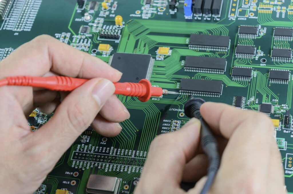
2. Continuity and Isolation Testing
This form of electrical testing ensures that all conductive paths on the PCB are correctly formed, and that there are no unintended connections between different circuits.
- Continuity Testing: This test checks that every electrical connection (trace) between two points on the PCB is intact, meaning no open circuits are present. It ensures that signals will flow as expected once components are installed.
- Isolation Testing: This method checks that no unintended connections (shorts) exist between different traces. Shorts can cause improper functionality or complete board failure. Isolation testing is critical, especially for high-density PCB designs, where close trace spacing can result in manufacturing defects.
These tests can be done manually with the use of multimeters or similar tools, but they are more commonly automated due to the complexity of modern PCBs. Automated testing methods for continuity and isolation are often more accurate and faster than manual approaches.
3. Flying Probe Testing
Flying probe testing is a versatile and cost-effective method for testing bare PCBs, especially useful for small or prototype batches. In this method, a set of probes, usually between two and six, “fly” over the PCB, contacting test points and pads to check for continuity and isolation.
The advantages of flying probe testing:
- No need for test fixtures: Unlike some other methods, flying probe testing does not require custom fixtures to hold the PCB. This reduces setup costs, especially for low-volume or prototype production.
- Flexibility: The test probes can easily adapt to different PCB designs, making this method suitable for a wide variety of board types and layouts.
- Cost-effectiveness: Flying probe testing is ideal for small production runs or high-mix low-volume manufacturing environments where creating custom fixtures is not economically viable.
However, flying probe testing may not be as fast as other automated methods, especially for large-scale production. The speed is limited by the physical movement of the probes.
4. Bed-of-Nails Testing
The bed-of-nails tester is a fixture-based testing method designed for high-volume PCB production. It consists of a bed of spring-loaded test pins (the “nails”) arranged in a grid. Each pin contacts a specific test point on the PCB, allowing the tester to simultaneously check for continuity, isolation, and other electrical characteristics.
Key advantages of the bed-of-nails testing method:
- High speed: Since all test points are contacted simultaneously, bed-of-nails testers can test PCBs much faster than flying probes. This makes it ideal for large-scale manufacturing.
- High accuracy: With a well-designed fixture, bed-of-nails testers can provide highly accurate measurements, identifying even small defects in the PCB.
Disadvantages of bed-of-nails testing:
- Fixture cost: The main drawback of this method is the cost of creating the custom test fixtures, which can be expensive and time-consuming. This cost is justified for high-volume production but is prohibitive for small batches or prototypes.
- Design limitations: As PCBs become more complex, with fine traces and high component density, designing and maintaining the test fixture becomes more challenging.
5. Automated Optical Inspection (AOI)
Automated Optical Inspection (AOI) is a method that uses high-resolution cameras and sophisticated image processing software to visually inspect PCBs. AOI can detect a wide range of issues, including:
- Misaligned layers.
- Broken or incomplete traces.
- Solder mask defects.
- Incorrect drill hole placement.
In the case of bare-PCB testing, AOI is mainly used to catch visual defects that might not be apparent during manual inspection. AOI systems are fast and accurate, making them well-suited for high-volume production environments where consistency is critical.
However, AOI cannot detect electrical problems, such as shorts or opens, and is usually combined with other testing methods to provide a comprehensive evaluation of the PCB’s quality.
6. Electrical Impedance Testing
As PCB designs become more advanced, impedance control becomes increasingly important, especially in high-speed circuits where signal integrity is critical. Impedance testing ensures that the impedance of specific traces matches the design specifications.
Impedance mismatches can result in signal reflections, noise, and reduced performance, especially in high-frequency applications like telecommunications and data networking. Impedance testing is often used in combination with other electrical testing methods to ensure that the PCB will perform correctly in its intended environment.
7. Automated X-ray Inspection (AXI)
While not commonly used for bare-PCB testing, Automated X-ray Inspection (AXI) can be employed in cases where internal defects in multi-layer PCBs are suspected. AXI can detect problems such as:
- Misaligned layers.
- Voids in vias or internal connections.
- Defects in buried or blind vias.
AXI is more commonly used during the assembly stage to inspect solder joints and component placement, but its use in bare-PCB testing is growing, especially for high-reliability applications.
Choosing the Right Testing Method
The choice of testing method depends on several factors:
PCB design complexity:
High-density boards with fine traces and multiple layers may require more advanced testing techniques, such as flying probe or impedance testing.
Production volume:
For low-volume production or prototypes, flying probe testing is typically more cost-effective, while bed-of-nails testing is more appropriate for high-volume manufacturing.
Cost considerations:
Some testing methods, such as bed-of-nails and AXI, require significant upfront investment in fixtures or equipment, which may not be justified for small production runs.
Speed and accuracy requirements:
High-speed production lines benefit from automated methods like bed-of-nails and AOI, while slower, more flexible methods like flying probes are ideal for early-stage development.
Conclusion
Bare-PCB testing is a critical step in ensuring the reliability of circuit boards. Through a combination of visual inspection, electrical testing, and automated techniques, manufacturers can detect and rectify defects early in the production process. As PCB designs continue to evolve, incorporating advanced testing methods such as impedance testing and AXI can help ensure that boards meet stringent performance requirements. By choosing the appropriate testing methods based on PCB design and production needs, manufacturers can produce reliable circuit boards that form the foundation of high-performance electronics.