
Printed Circuit Boards (PCBs) form the foundation of most modern electronic devices. As electronic products have evolved, so have the demands for more compact and intricate designs, making the adoption of double-sided PCBs a key advancement in PCB design. These boards not only improve functionality but also support more complex circuits while maintaining a manageable size. This article explores how double-sided PCBs enhance circuit complexity and functionality and why they are increasingly crucial in the electronics industry.
Understanding Double-Sided PCBs
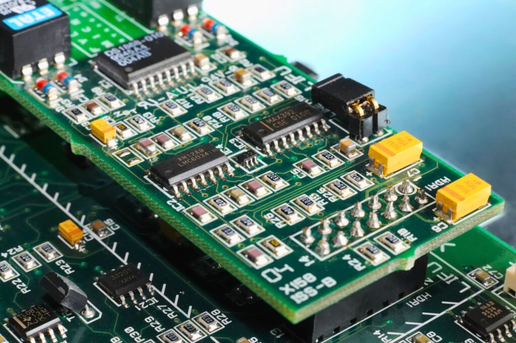
A double-sided PCB consists of two copper layers — one on the top and one on the bottom of the board. This allows for the placement of components on both sides, doubling the area available for circuit routing compared to single-sided boards. The two copper layers are connected through vias (small holes drilled through the PCB and plated with conductive material), enabling electrical connections between components on different sides of the board.
Advantages of Double-Sided PCBs
- Increased Component Density
Double-sided PCBs allow for more components to be mounted on the same board size, significantly increasing circuit density. This is essential for modern devices like smartphones, wearables, and IoT devices, where space is limited, but the functionality is complex. - Improved Functionality
With components on both sides and more interconnections, engineers can design more complex circuits that support additional features. For instance, double-sided PCBs can handle more advanced electronic systems, such as RF circuits, power management modules, and microcontrollers, improving overall functionality. - Compact Design
The ability to utilize both sides of the board means designers can create smaller and more compact circuits without sacrificing performance. This is particularly useful for portable devices, where size constraints are critical, and efficiency is paramount. - Cost-Effectiveness
While double-sided PCBs are more complex to manufacture than single-sided boards, they are more cost-effective than multilayer PCBs, especially for medium-complexity designs. This makes them an ideal solution for products that require enhanced functionality but have budget constraints. - Flexibility in Design
Double-sided boards provide more flexibility in routing traces and placing components. Designers can optimize signal paths, reduce electromagnetic interference (EMI), and improve overall circuit performance by strategically placing components on both sides of the PCB.
The Role of Vias in Double-Sided PCBs
Vias are a crucial component in PCB design, especially for double-sided boards. They allow electrical signals to pass between the top and bottom layers, effectively increasing the number of routing options. There are several types of vias commonly used in double-sided PCBs:
Through-hole vias:
These are the most common type of vias, connecting the top and bottom layers by drilling completely through the board.
Blind vias:
These connect an outer layer with an inner layer without passing through the entire board (used in multilayer PCBs, but also seen in advanced double-sided designs).
Buried vias:
These connect internal layers only and are usually found in multilayer boards, though some complex double-sided designs may utilize them as well.
Strategic via placement is essential to optimize space and ensure a clean signal flow in double-sided PCB designs.
Double-Sided PCBs in Modern Applications
The rise of double-sided PCB design has enabled the development of advanced consumer electronics, industrial systems, and medical devices. Here are a few examples:
- Consumer Electronics: Devices such as smartphones, laptops, and gaming consoles rely on double-sided PCBs for their compact form factors and high performance.
- Automotive Industry: Modern cars use advanced electronic systems for engine control, infotainment, and safety features, all of which are supported by double-sided PCBs that handle complex circuitry in a confined space.
- Medical Devices: Compact medical equipment like pacemakers, hearing aids, and diagnostic devices use double-sided PCBs to integrate multiple functions within small form factors.
- Industrial Automation: Double-sided PCBs play a critical role in industrial automation, where space is often constrained, but systems require intricate circuit designs for control systems, sensors, and communication modules.
Challenges in Double-Sided PCB Design
Despite their advantages, designing double-sided PCBs comes with its challenges. Increased complexity requires careful planning and precision in routing, component placement, and layer interconnections. Designers must also consider factors like heat dissipation, signal integrity, and potential crosstalk between traces.
Moreover, manufacturing double-sided PCBs can be more complex and costly than single-sided boards due to the need for via drilling, lamination, and more intricate etching processes. However, with modern manufacturing techniques, the cost has become increasingly manageable, making double-sided PCBs a preferred choice in many applications.
Conclusion
Double-sided PCBs have significantly enhanced the capabilities of PCB design, enabling more complex and functional circuits in compact devices. By allowing components and interconnections on both sides of the board, designers can create sophisticated products that meet the demands of modern electronics. As the need for more powerful and smaller devices continues to grow, double-sided PCBs will remain a critical technology in advancing electronic design and functionality.