
Design for manufacturability (DFM) turns early engineering choices into faster builds, higher yields, and lower total cost. If your team works in pcb design, embedded electronics, or electromechanical products, applying DFM early can prevent weeks of rework and keep unit economics healthy. This guide walks through field-tested methods—from part selection and layout rules to stencil tuning and panel decisions—so your next build moves through SMT, test, and final assembly with fewer surprises.
What is DFM and why it matters
DFM is the discipline of shaping a product so it can be produced repeatedly, with stable quality and predictable cost, on real factory lines run by real people and machines. It connects design choices to actual process limits: component tolerances, pick-and-place accuracy, reflow profiles, inspection capability, AOI rules, test coverage, packaging, and logistics. Teams that apply DFM treat manufacturing as a first-class requirement, not a late gate review.
There are five business reasons teams invest in DFM: 1) fewer design spins by catching production blockers before tooling and NRE are committed, 2) higher first-pass yield on pilot and ramp, 3) shorter lead time from order to ship due to fewer stoppages, 4) more stable BOMs with risk-managed alternates, and 5) lower total landed cost through panel efficiency, touch-time reduction, and improved test coverage. Good DFM shortens the distance between “works on bench” and “ships at scale.”
DFM spans three layers. First, product architecture choices that influence process steps (connectors, form factor, interconnects, materials). Second, detailed rules for PCB layout, stencil, solder mask, component footprints, and panelization. Third, operational practices: checklists, factory feedback, SPC on yields, and ECO hygiene. Treat all three together to avoid local optimizations that create new bottlenecks elsewhere.
Component selection and sourcing
The cheapest component on paper can be the costliest in production if it drives low yield, custom fixtures, or intermittent field issues. Build your Approved Vendor List (AVL) with these guidelines:
Availability and lifecycle. Prefer active parts with multiple authorized distributors and published longevity roadmaps. Scrutinize “NRND” and “EOL” flags; carry at least one vetted alternate for every single-sourced passive value and common ICs (LDOs, op-amps, logic). Validate alternates with identical or compatible footprints to avoid layout spins.
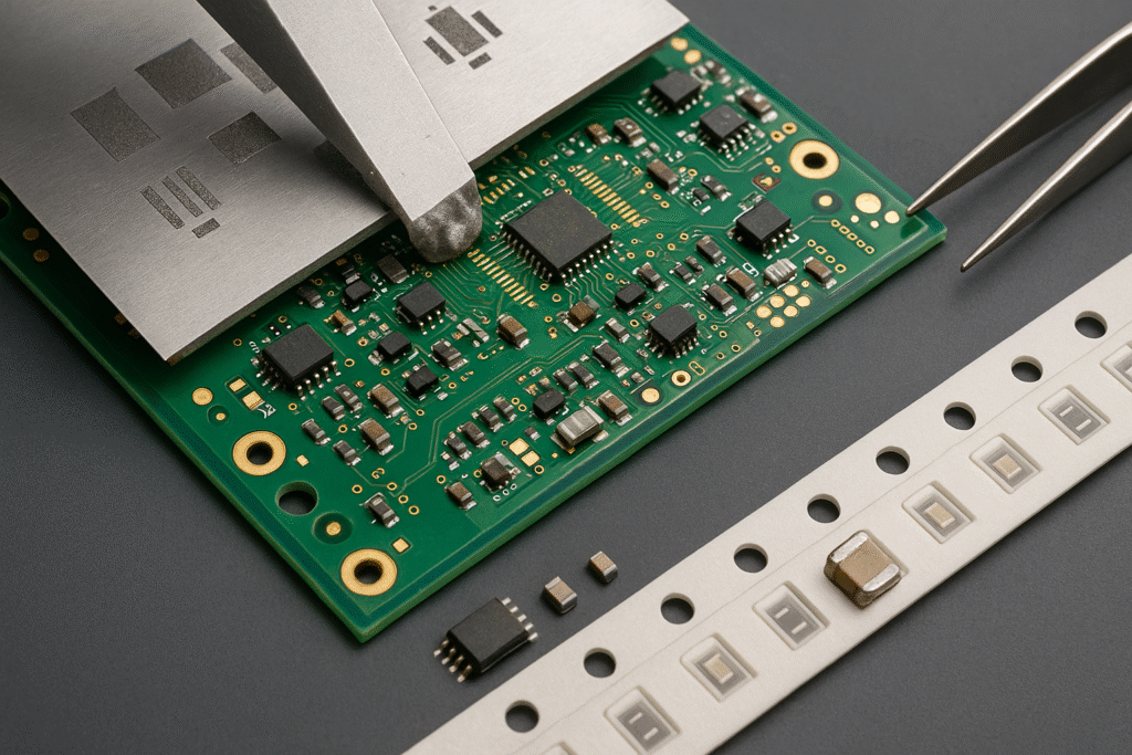
Package types. For high-mix builds and small-batch runs, pick packages with stable pick-and-place performance: 0402/0603 for passives (0201 only where density forces it), DFN/QFN with exposed pad for power ICs, and leaded packages where rework is likely. BGA brings density but adds X-ray time and rework difficulty; allocate budget for test fixtures and skilled rework if you rely on fine-pitch BGA.
Moisture sensitivity and handling. Note MSL ratings from datasheets. MSL3+ parts require baking and controlled floor life after opening; this affects factory scheduling. Work with the CM to align packaging quantities with feeders to cut setup waste.
Regulatory and regional constraints. Confirm UL94 flammability, halogen content, or automotive grade needs (AEC-Q100/Q200) upfront. If you ship into harsh environments, derate by temperature and voltage margins tighter than the typical consumer profile.
Cost and inventory risk. Use parametric searches to find pin-compatible families across multiple brands. Lock in alternates early and trace them in your PLM/ERP so buyers are not scrambling during shortages. Small variations (e.g., tighter tolerance, higher voltage rating) that cost pennies may avoid a full redesign later.
Electromechanical choices. Select connectors that match automated processes: pick SMT headers with hold-downs over through-hole headers when possible, and avoid odd board-edge orientations that create manual insertion steps. For switches, LEDs, and antennas, verify keepouts, mechanical height, and reflow compatibility to prevent secondary hand-solder operations.
PCB layout considerations for assembly
Assembly-friendly layout lowers defects without hurting performance. Work with your CM’s DFM ruleset (they often provide a PDF or IPC-based checklist). Key points:
Land pattern accuracy. Base footprints on manufacturer land recommendations and IPC-7351, then tune for your CM’s stencil thickness and solder paste type. For QFN, use segmented thermal pads with via-in-pad plated over (VIPPO) or tented vias to prevent paste wicking.
Component orientation. Align most components to a common rotation (e.g., 0° or 90°) to speed programming and reduce placement mistakes. Keep reference designators readable and consistent.
Spacing and keepouts. Maintain clearances for AOI camera angles and rework tools. Leave at least 1 mm around tall parts for nozzle access and hot-air rework. Respect copper-to-edge distance for routing, and add mechanical keepouts under connectors that experience insertion force.
Thermal balance. Avoid large copper asymmetry around fine-pitch parts; big pours on one side of a pad can cause tombstoning and skew during reflow. Use thermal relief spokes on through-hole pads to prevent cold joints.
BGA and fine-pitch routing. Decide early between via-in-pad (VIPPO) and dog-bone fanout; VIPPO improves density and signal quality but adds cost and requires filled/planarized vias. Keep escape routing uniform and match solder mask expansion to your CM’s registration tolerance to prevent solder shorts.
Testability. Place test pads for power rails, reset lines, programming interfaces (SWD, JTAG, UART), and high-risk nets. Reserve connector footprints for optional test headers on pilot builds. Plan boundary scan chains for dense BGA devices and maintain access after final enclosure assembly.
Silkscreen and polarity. Mark pin-1, cathode/anode, and switch orientation with unambiguous shapes, not just text. Reinforce with copper or mask shapes when silkscreen may be clipped by keepouts.
Stencil design for solder paste
Stencil choices directly influence solder volume, wetting, and defect rates.
Material and thickness. A 100–130 μm laser-cut stainless stencil fits most mixed-tech boards; adjust by part mix. Thinner stencils (80–100 μm) help with 0.4 mm pitch and 01005 passives but may starve large thermal pads. Thicker stencils (150 μm) feed big power pads but risk bridging on fine pitch.
Aperture reductions. For QFN thermal pads, reduce total paste area to ~50–70% using windowpane patterns to prevent float and squeeze-out. For small passives prone to tombstoning, shrink the smaller pad’s aperture or balance copper to match thermal mass.
Aperture shapes and corner radii. Rounded corners improve paste release; trapezoidal walls (from electroform or nano-coatings) reduce clogging. Where voiding matters (power pads), use multiple smaller apertures spaced to promote outgassing.
Step-down/step-up. Consider stepped stencils if your design mixes 0.4 mm pitch BGAs and large power pads. Work with your CM to decide whether two paste prints or selective dispense is better than a stepped tool on early pilots.
Paste type and storage. Match paste alloy and viscosity to your reflow process (SAC305 vs low-temperature alloys, no-clean vs water-soluble). Control paste age and storage per vendor data; expired paste is a silent yield killer.
Panelization strategies
Panelization affects throughput, depanel stress, and scrap.
Board orientation and array size. Choose an array that fits the stencil printer and pick-and-place bed (often 18×24 in or 20×24 in panels). Keep array weight manageable for operators and allow for fiducials, tooling holes, and break-off rails.
Rails and mouse-bites. Provide 5–10 mm rails on all sides for conveyor belts. Place mouse-bites with small tabs and drill perforations that break cleanly without tearing solder mask near edge connectors. For brittle laminates or tight tolerances, use V-scoring along straight edges and keep parts away from the score line.
Component overhang and tall parts. Avoid parts that stick beyond the board outline inside the array; they can hit adjacent boards during reflow or AOI. If unavoidable, stagger placement between rows.
Labeling and traceability. Reserve space for panel and unit-level barcodes or QR codes. Place labels where AOI cameras can see them and where rework won’t remove them. Consider laser marking for high-temp or chemicals exposure.
Co-paneling variants. If you must combine variants, maintain identical outlines and shared fiducials. Segregate BOM differences to avoid feeder swaps between units in the same run.
Solder mask and fiducial placement
Solder mask and fiducials guide machines and protect your finish.
Solder mask dam and expansion. Keep mask dams between pads to reduce solder bridging; a 75–100 μm dam is typical where registration allows it. Set mask expansion values to avoid exposing copper slivers that trigger AOI false calls.
Tenting and via handling. Tent small vias under QFN to reduce paste wicking. For via-in-pad solutions that require filling, specify epoxy fill and copper cap in your fab notes and talk through flatness targets with the board house.
Global and local fiducials. Place at least three global fiducials on the panel rails and two local fiducials near fine-pitch parts (BGA, QFN). Keep them free of solder mask with a clear ring around each. Do not place silkscreen across fiducials.
Finish compatibility. Choose a surface finish that matches your assembly process: ENIG for fine pitch and flatness, HASL for low-cost larger pitch, immersion silver for signal integrity on RF traces (while managing tarnish risks), or ENEPIG when gold wire-bonding or multiple reflows are expected.
Standardization of footprints and packages
Footprint drift is a common source of rework. Standardize to reduce effort and risk.
Central library. Maintain a single library with verified footprints and 3D models. Lock naming conventions (MFR_PN_PACKAGE_PINCOUNT) and metadata fields (height, polarity, paste options). Gate new parts through a librarian review before they land in production designs.
IPC vs vendor patterns. Start with IPC-7351 footprints but compare against vendor-specific land patterns, especially for QFN/BGA and odd connectors. Document differences and rationale so the next project doesn’t repeat the same work.
Variants and alternates. Where alternates exist, design a “combo” footprint that accepts both pin-compatible options (e.g., SOT-223 and DPAK for linear regulators) if space allows. That resilience can rescue a build when one package goes short.
Assembly notes and 3D checks. Keep body outlines accurate for enclosure fits and height stacking. Use 3D clearance checks to catch clashes with housings, shields, and fasteners well before tooling is cut.
Handling tight tolerances and shrinkage
Precision starts long before machining and molding. Electronics that mate with plastics, metals, and seals must budget for both fabrication tolerance and process shrinkage.
Board fab tolerances. Call out finished thickness with tolerance (e.g., 1.6 mm ±10%). Work with the fab to set drill sizes and plating allowance so final holes match press-fit or mechanical fastener specs. If press-fit pins are used, follow manufacturer hole size charts with tolerance stack in mind.
CTE and thermal exposure. FR-4 expands with heat; reflow cycles and conformal coating cure can shift dimensions. Keep critical slots and mounting holes referenced from a common datum and provide slightly elongated holes where alignment to a chassis is needed.
Plastic parts. For injection molded enclosures, apply shrink factors per resin (ABS, PC, PA6, etc.) and gate location. Leave generous draft angles and fillets to reduce sink and warpage. Validate snap features with multiple mold flow simulations and pilot builds, not just CAD assumptions.
Gasket and seal compression. For IP-rated assemblies, set compression ranges for gaskets and verify with actual torque values and screw retention features (boss design, metal inserts). Over-compression ruins ingress protection; under-compression leaks.
Stack-up variability. Use controlled-impedance stack-ups with documented prepreg and core options. If a substitute dielectric is needed due to supply, validate impedance impact and tweak trace widths accordingly. Lock the stack-up in the fab notes to avoid silent substitutions.
DFM reviews and checklists
Checklists turn tribal knowledge into repeatable results. A structured DFM review catches issues faster than ad-hoc comments.
Inputs. Collect fab notes, assembly notes, stack-up, paste layer, 3D step files, enclosure CAD, test plans, and BOM with alternates. Missing inputs delay sign-off.
Scope. Review items in themed passes: 1) layout and land patterns, 2) stencil and paste, 3) panel and fiducials, 4) test and programming access, 5) mechanical fit and fasteners, 6) regulatory and safety marks, 7) labeling and traceability, 8) shipping/packaging.
Roles. Assign a lead reviewer and domain reviewers (layout, SI/PI, mechanical, test, manufacturing, quality). Time-box the session and follow with action items recorded as ECOs or ticketed tasks.
Evidence. Where a rule deviates by design (e.g., tight clearance for RF), attach the rationale and validation data so production teams are not left guessing during a stop-ship event.
Sign-off gates. Make DFM approval a release criterion equal to schematic and layout approval. If something ships without DFM sign-off, record a waiver approved by engineering and operations leadership.
Collaboration with contract manufacturers
A strong relationship with your contract manufacturer (CM) is the multiplier for all of the above.
Start early. Share early Gerbers, 3D CAD, and a preliminary BOM for a free DFM pass. Small comments at this stage can prevent hours of rerouting or mechanical redesign. Ask the CM for their standard ruleset and stencil preferences, then tailor your design to it.
Be clear on build intent. State whether the run is EVT, DVT, PVT, or mass production, and which tests are mandatory at each phase. Clarify acceptable substitutions and whether the CM can draw from their in-house stock for passives.
Golden samples and fixtures. Provide a golden unit for AOI programming and operator training. Invest in durable test fixtures and label storage so they are not rebuilt every run. If you need in-circuit test (ICT), engage fixture design while layouts are still movable; dense boards without ICT pads drive up functional test time.
Change control. Route all changes through a documented ECO process. Share revision histories with the CM and include clear “what changed” notes, not just a new ZIP. Keep a standing weekly call during ramp so small issues don’t pile up into a line stop.
Quality metrics. Track first-pass yield, top defect Pareto, touch-time, and fallout causes. Ask the CM to separate solder-related defects from part quality issues; each has a different fix. Review X-ray images of BGA/QFN on early lots and approve reflow profiles with measured thermocouples on your board, not a generic coupon.
Continuous improvement and feedback loops
Treat each build as data. A few habits turn production noise into better designs:
Root cause analysis. For every high-frequency defect (tombstoning, bridges, opens, voids), log the suspected cause and the confirmed fix. Tie each to a future design rule or stencil tweak.
DFX retrospectives. After EVT/DVT/PVT, hold a 60-minute review on what to change in the next rev: DFM (manufacturability), DFT (testability), DFA (assembly), DFS (serviceability). Turn each insight into a rule, library update, or checklist item.
SPC on key parameters. Track Cp/Cpk for hole sizes, board thickness, and solder paste deposition volume where applicable. Trends warn you before yields crash.
Supplier scorecards. Rate CMs and board houses on delivery, yield, responsiveness, and paperwork accuracy. Share this transparently; it motivates the right behaviors without micromanagement.
Documentation hygiene. Keep fab and assembly notes current. When you change a finish, stencil thickness, or panel array, roll the revision and log the reason so future teams understand the history.
Practical DFM best practices by topic
To close the loop, here is a condensed set of field-ready practices you can apply on the next build.
BOM and parts
• Prefer active, multi-source parts with pin-compatible alternates baked into the AVL.• Limit exotic packages unless density demands them; choose rework-friendly options for risky circuits.• Add moisture-sensitivity handling notes for MSL3+ items in assembly docs.• Buy reels in feeder-friendly quantities to reduce setup waste and line stops.
Layout and footprints
• Use vendor land patterns as the starting point; document deviations and the reason.• Balance copper around small passives; match pad sizes to reduce tombstoning.• Keep at least 1 mm clearance around tall parts for nozzle and rework tool access.• Place programming and test access facing the board edge or a removable section of the enclosure.
Stencil and paste
• Choose stencil thickness to fit the finest pitch on the board, then compensate large pads with windowpane apertures or stepped regions.• Use rounded apertures for better paste release; consider nano-coatings when fine features clog.• Requalify paste types when you change reflow profiles or finishes.
Panel and handling
• Design arrays to standard printer frames and conveyor widths; keep rails clean and add tooling holes.• Protect sensitive edges from V-score tear-out with component keepbacks.• Provide clear panel and unit-level labels for traceability through AOI and test.
Solder mask and finish
• Maintain mask dams where registration allows; avoid slivers that trigger AOI flags.• Tent or fill vias under QFN/BGA based on risk of wicking and planarity needs.• Match finish to pitch and reflow cycles (ENIG for fine pitch, HASL for economy, ENEPIG for wire-bond or multiple reflows).
Test and programming
• Add boundary scan chains and accessible headers for critical ICs; keep them reachable after assembly into the enclosure.• Define a minimal functional test plan for EVT and scale toward ICT or bed-of-nails as volumes rise.• Include golden units and self-test scripts; keep them under revision control.
Mechanical and tolerance
• Call out datums and hole tolerances with real manufacturing numbers from suppliers.• Budget for CTE and cure shifts through slots and elongated holes where alignment matters.• Validate gasket compression and screw torque with physical trials, not just CAD.
Operations and quality
• Run formal DFM reviews with checklists and roles; record waivers and data to back exceptions.• Track first-pass yield and Pareto of defects; feed fixes into the library and rules.• Keep a weekly build call during ramp and maintain tight ECO control.
Example DFM checklist (starter template)
Use this as a base and adapt to your line and product:
BOM and parts
[ ] All passives have vetted alternates with verified footprints[ ] No NRND/EOL items without approved waiver and lifetime buy plan[ ] Moisture sensitivity notes captured for MSL3+ parts[ ] Connector mating parts and orientations confirmed
Layout and assembly
[ ] All fine-pitch parts have local fiducials[ ] Polarity and pin-1 marks visible after assembly[ ] 1 mm clearance around tall components for rework[ ] Heat-sensitive parts isolated from hot spots and keepouts observed
Stencil and paste
[ ] Stencil thickness matched to finest pitch[ ] QFN thermal pads window-pane apertures sized to 50–70%[ ] Small passive tombstoning risk addressed by pad/paste balance[ ] Paste type and alloy listed in assembly notes
Panel and labels
[ ] Standard rails added with tooling holes and global fiducials[ ] Mouse-bites or V-score specified; sensitive edges protected[ ] Unit and panel barcodes placed for AOI visibility
Test and programming
[ ] ICT/bed-of-nails strategy defined or deferred with plan[ ] Boundary scan chain accessible; programming header placed[ ] Golden unit ID recorded; fixture drawings under version control
Mechanical and finish
[ ] Stack-up locked; impedance targets shared with board house[ ] Hole sizes and tolerances match fasteners and press-fit data[ ] Surface finish selected for pitch and reflow count; no silent substitutions
Quality and documentation
[ ] Reflow profile approved with on-board thermocouple data[ ] AOI and X-ray inspection plan defined for BGA/QFN[ ] ECO process defined; latest Gerbers/STEP/BOM shared in one package[ ] CM’s feedback logged with actions and owners
DFM across product life cycle: EVT → DVT → PVT → mass production
EVT (engineering validation test) focuses on architecture, risk circuits, and quick-turn proofs. Accept some hand rework and bodge wires but still apply a minimum DFM bar: standard footprints, practical test headers, and stencil-friendly paste. Capture every rework and rationale.
DVT (design validation test) locks the design for performance and reliability. Run full DFM, add ICT pads if volumes justify them, and validate reflow with real thermocouple data on your board. Tune stencils and reflow profile based on AOI/X-ray feedback.
PVT (production validation test) proves the line. Freeze panel arrays, labels, packing, and test fixtures. Measure first-pass yield across multiple lots and days to catch line-to-line variation. Lock work instructions and quality gates.
Mass production is about stability. Control changes tightly, watch SPC trends, and refresh fixtures and stencils based on wear. Treat supplier audits and periodic process reviews as normal hygiene, not fire drills.
Risk hot-spots to watch
• Fine-pitch BGA without local fiducials or with mask openings that are too aggressive• QFN center pads with full-coverage paste causing float and shorts• Odd connectors needing manual soldering due to shadowing or thermal mass• Components too close to V-score or mouse-bite lines leading to cracks after depanel• Lack of test access driving long functional test times and high NPF (“no problem found”) returns• Moisture-sensitive devices baked or reflowed outside floor-life limits• Alternate parts added on the fly without land-pattern or parametric validation
Documentation set that speeds factory onboarding
A tidy handoff saves days: 1) Fabrication package (Gerbers or ODB++, stack-up, drill files, fab drawing with notes). 2) Assembly package (centroid/XY, BOM with alternates and supplier links, paste layer, assembly drawing, reflow guidance). 3) Test package (schematic PDF, programming images, test plan, limits, fixture drawings, sample commands). 4) Mechanical package (STEP of PCB and major parts, enclosure STEP, fastener specs, torque targets). 5) Quality package (label samples, inspection criteria, special process notes such as conformal coat or underfill).
Conclusion
Good DFM is not glamorous; it is a set of steady habits that pay off at every build. Start with resilient part choices, use assembly-friendly footprints, balance paste with smart stencil work, design arrays for the actual machines on the line, and keep feedback flowing from factory to library. When your product moves from prototype to sustained production, these habits remove uncertainty, improve yields, and protect margins. Treat each lot as data, roll the lessons into your rules and libraries, and your next program will start ahead of the curve.