
Nowadays, all electrical and electronic manufacturers try their best to sell high-performance products. For this, they ensure that all design standards and rules are met. Electronic devices must have the required EMC/EMI certificates when they come to the market. EMC/EMI are crucial testing standards, along with all other rules and standards.
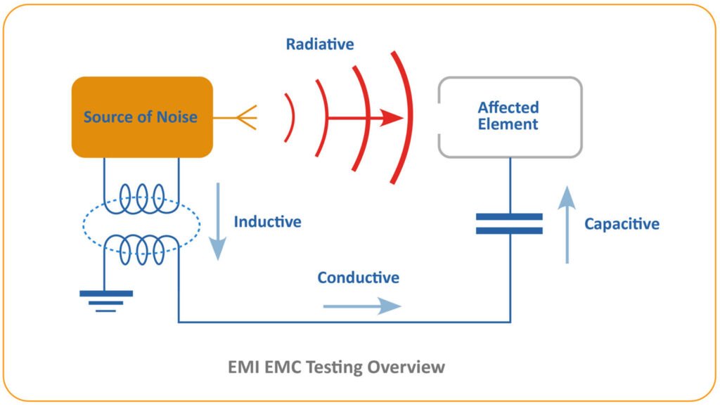
EMI stands for Electromagnetic Interference. It refers to the noise signals generated by an electric circuit that interferes with nearby devices. As a result, device operation is disturbed.
Electromagnetic Compatibility is the ability of a circuit to operate correctly even under the interference of noise signals.
What Causes EMI Problems?
- Electromagnetic fields produced by electric current cause harmful effects on the working of nearby devices.
- EM emissions increase when there is an increase in the loop or coil area. EM emissions also increase with the rate of current changes.
- Mismatched impedance also creates EMI problems.
- Poor capacitance decoupling and high-frequency traces also result in EM emissions.
- High-rate transmission signals and clock signals can also cause EMI problems.
How to Design PCB to Make It EMC Compliant?
If you want your circuit board to be EMC compliant, it must have the following characteristics:
- It shouldn’t interfere with other boards
- Its immunity should be strong against the emission of other systems
- It doesn’t interfere with its operations
It means PCB design can help reduce EMI. There are three main sources of EMI.
Here we’ll discuss only two. The 3rd source of EMI is external EMI.
Electronic Components
Components with higher power consumption, like switching components, antennas, and transmitters, generate EM emissions. Following precautions can help you limit EMI associated with electronic components.
- Choose low-power consumption components
- Use SMD device because it’s suitable for high-frequency applications
- Use analog components to group and isolate signal-processing components
- Use Faraday cage to separate sub-circuits. It prevents radiation emissions around the board.
The second component is:
PCB Layout
It’s possible to reduce the EMI problems in PCBs by considering design traces, PCB layers arrangement, grouping sensitive components, Ground Plane, Shielding, controlled impedance, and Decoupling capacitor. Let’s briefly explain the role of each of them.
Traces
They’re the conductive paths of the PCB surface to transfer signals between electronic components and flow electric current. Copper is the most commonly used trace material.
PCB Layers
EMC performance mainly depends on layer arrangement in PCB. There should be a proper ground, power, and signal layer for the best EMC performance.
Ground Plane
The role of a ground plane is to reduce noise and EMI interference and voltage and signal return.
Decoupling Capacitor
The decoupling capacitance technique in high-speed circuits can significantly reduce EMI in power rails. Using a bypass capacitor and connecting it to the ground plane can help reduce EMI.
Impedance Matching
Increased conducted emissions in the circuit cause EMI problems in a circuit. Mismatching impedance is caused in high-frequency circuits. RF termination technique can help obtain impedance matching.
Shielding
As mentioned earlier, the third source of EMI emissions is External EMI. Shielding plays its part in protecting the board from external EMI. An enclosure is made of magnetic or conductive materials.
In addition, it covers the entire board. Part of this shielding is connected to the ground.

Conclusion
Considering some applicable rules in PCB design can help electronics manufacturers get the best EMI/EMC performance. It’s impossible to eliminate EMI, but by following the guidelines mentioned above, you can reduce EMI. Moreover, you can get the help of Arshon Technology for PCB design.