
Understanding how PCBA manufacturing works is essential for anyone involved in electronics, from product designers to manufacturers. PCBA, or Printed Circuit Board Assembly, is the process of populating a bare PCB with electronic components to create a fully functional device. From early pcb design stages to soldering and inspection, every step impacts quality, cost, and performance. This article provides a complete walkthrough of PCBA manufacturing, highlighting each stage in detail and offering insights into the technologies that make modern electronics possible.
Basics of PCB Fabrication
Before components can be assembled, the bare PCB must be fabricated. The process starts with pcb design, where engineers create circuit layouts using software like Altium, KiCad, or Cadence. The layout defines copper traces, vias, and pads that interconnect components. Key steps in PCB fabrication include:
- Substrate preparation: Most PCBs use FR-4 (fiberglass epoxy) as a base material.
- Copper lamination: Copper foil layers are bonded to the substrate.
- Imaging and etching: Circuit patterns are transferred and excess copper is etched away.
- Drilling: Holes for vias and through-hole components are drilled.
- Plating: Copper plating coats drilled holes to create conductive pathways.
- Solder mask and silkscreen: Protective solder mask is applied, and component labels are printed.
The resulting bare board provides the foundation for assembly.
Applying Solder Paste with Stencils
The first step in PCBA assembly is applying solder paste. Solder paste is a mixture of tiny solder particles and flux that temporarily holds components in place before reflow.
- Stencil alignment: A stainless steel stencil is placed over the PCB.
- Paste application: A squeegee spreads solder paste across the stencil, filling openings where pads are exposed.
- Precision control: Automated stencil printers ensure accuracy, as improper paste application can cause shorts or cold joints.
This step sets the stage for accurate component placement.
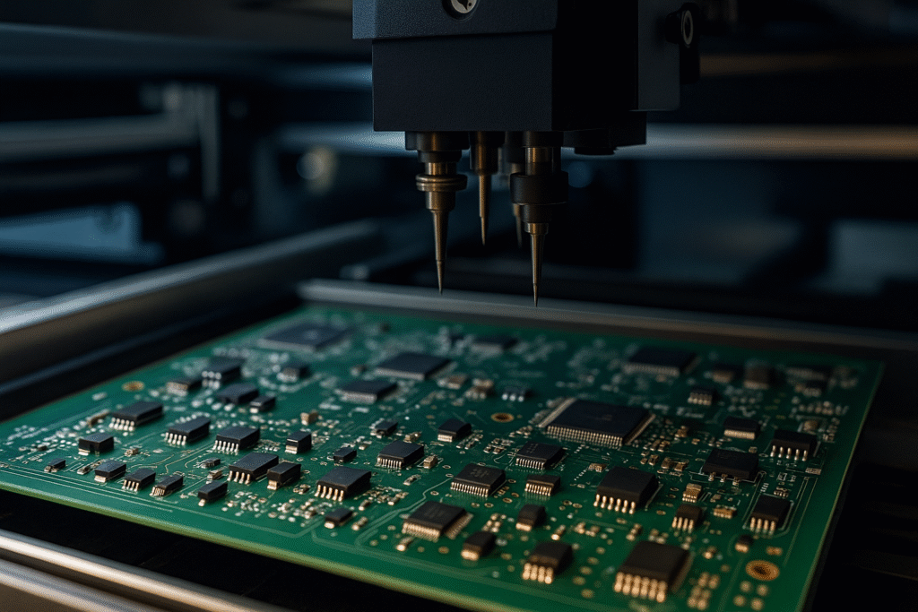
Automated Component Placement
Surface-mount technology (SMT) dominates modern PCBA. Automated pick-and-place machines handle this step:
- Component feeders: Machines draw components from reels or trays.
- Vision systems: Cameras identify component orientation and location.
- Placement: High-speed robotic arms place components onto solder-paste-covered pads.
Modern machines place tens of thousands of components per hour with micron-level precision. This automation allows consumer electronics, IoT devices, and medical devices to be manufactured at scale.
Reflow vs. Wave Soldering Techniques
Once components are placed, they must be soldered permanently. Two major soldering methods are used:
Reflow Soldering
- Used for SMT components.
- Boards pass through a reflow oven with controlled heating zones.
- Solder paste melts and solidifies, forming permanent joints.
- Nitrogen environments are sometimes used to reduce oxidation.
Wave Soldering
- Primarily for through-hole components.
- Boards pass over a wave of molten solder.
- Solder adheres to exposed pads and component leads.
- Common in power electronics and mixed assembly.
Many PCBs require both methods, especially in mixed-technology boards.
Inspection Methods: AOI, X-ray and ICT
Inspection ensures quality and prevents defects:
- AOI (Automated Optical Inspection): Cameras detect missing, misaligned, or poorly soldered components.
- X-ray inspection: Critical for BGAs and hidden solder joints where AOI cannot see.
- ICT (In-Circuit Testing): Electrical probes test functionality by measuring resistance, capacitance, and signals.
By combining these techniques, manufacturers catch both visual and electrical faults.
Through-Hole Soldering and Mixed Assembly
While SMT dominates, through-hole technology is still used for:
- Connectors.
- Large power components.
- Mechanical reinforcement.
Manual soldering or wave soldering completes this step. Mixed assembly involves both SMT and through-hole processes on the same board, requiring careful process sequencing.
Cleaning and Conformal Coating
After soldering, boards may be cleaned to remove flux residues that can cause corrosion or shorts. Cleaning methods include aqueous cleaning, solvent-based cleaning, or no-clean flux that leaves safe residues. For harsh environments, conformal coatings are applied to protect PCBs from moisture, dust, and chemicals.
Functional Testing and Quality Control
Before shipping, boards undergo functional testing:
- Boundary scan: Checks interconnections between ICs.
- Power-on test: Ensures the board powers up correctly.
- Functional verification: Simulates end-use conditions.
These tests ensure the final product meets performance and safety requirements.
Challenges in PCBA Manufacturing
Common challenges include:
- Miniaturization: Smaller components and higher densities increase difficulty.
- Thermal stress: Excessive heating during reflow can damage components.
- Supply chain variability: Component shortages can require design substitutions.
- Defects: Tombstoning, bridging, and voids must be controlled.
Solutions involve advanced process monitoring, design-for-manufacturing (DFM) practices, and close supplier collaboration.
The Role of PCB Design in PCBA Success
Effective pcb design is the foundation of successful PCBA. Key practices include:
- Clear pad design: Prevents solder bridging.
- Trace width optimization: Ensures proper current handling.
- Thermal relief patterns: Improve solderability of large copper areas.
- Component spacing: Facilitates automated placement and inspection.
- Design for testability (DFT): Allows easier ICT and functional testing.
Good design reduces manufacturing defects and lowers production costs.
Environmental and Regulatory Considerations
Modern PCBA manufacturing complies with strict regulations:
- RoHS (Restriction of Hazardous Substances): Limits use of lead and other harmful materials.
- REACH compliance: Ensures safe chemical use.
- ESD protection: Prevents damage to sensitive ICs during assembly.
Sustainability efforts also focus on reducing waste, recycling materials, and improving energy efficiency.
Future Trends in PCBA Manufacturing
The future of PCBA will involve:
- AI-driven process control: Real-time defect prediction.
- Industry 4.0 integration: Smart factories with IoT-enabled machines.
- Miniaturization: Even smaller PCBs for wearables and medical devices.
- Advanced materials: High-speed laminates for 5G and aerospace.
- Automation expansion: Robots handling mixed assembly tasks.
These trends will push PCBA to new levels of efficiency and capability.
Conclusion
Understanding how PCBA manufacturing works requires exploring every step from pcb design to final testing. The process involves precise application of solder paste, automated placement, reflow and wave soldering, thorough inspection, and rigorous functional testing. Success depends on strong design practices, advanced automation, and adherence to regulatory standards. As technology continues to evolve, PCBA will remain at the center of modern electronics innovation, powering everything from smartphones to autonomous vehicles.