
Energy Harvesting
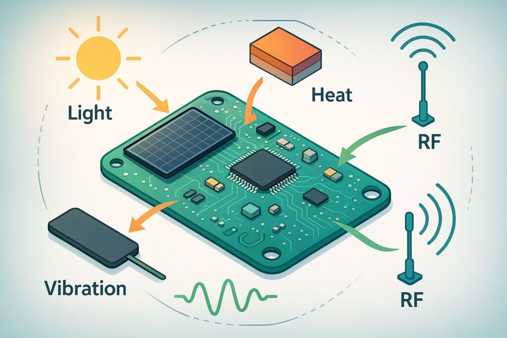
Energy harvesting converts ambient energy—light, heat, vibration, RF, or fluid flow—into electrical power that can drive low‑consumption electronics. Doing so removes or extends batteries, slashes maintenance, and enables autonomous sensors in hard‑to‑reach locations. For a PCB designer, the transition from finite battery packs to renewable micro‑sources demands a new mindset: ultra‑low leakage currents, sub‑microamp quiescent regulators, efficient power routing, and robust protection against unpredictable input voltages.
A modern energy‑harvesting node typically includes: a transducer (solar cell, thermoelectric generator, piezo patch), an energy‑conditioning path (rectifier, boost or buck converter, maximum‑power‑point‑tracking logic), an energy buffer (super‑capacitor or thin‑film battery), a low‑power microcontroller or sensor hub, and a wireless transmitter. Each block imposes its own PCB requirements—from Kelvin‑sense routing of μ‑ohm current shunts to RF impedance control—and all must coexist in a footprint smaller than a credit card and often thinner than a millimeter.
Overview of Technologies
1. Photovoltaic (PV) mini‑panels are the most mature option. Flexible monocrystalline silicon or perovskite thin films deliver 5–30 mW/cm² under indoor lux levels. PCB implications: large footprint mounting pads, reverse leakage protection diodes, and angled board outlines for optimal light capture.
2. Thermoelectric Generators (TEGs) exploit temperature gradients (ΔT). P‑ and N‑type semiconductor couples produce tens of millivolts per degree Celsius. Designers must add low‑startup boost ICs (down to 15 mV) and thermally conductive paths—aluminum IMS substrates or copper planes—between hot and cold sides.
3. Piezoelectric & Electrodynamic Harvester devices capture vibration or mechanical strain, generating high open‑circuit voltages (10–90 V) but microamp currents. PCBs need high‑voltage tolerant rectifiers, asymmetrical CLC filters to suppress resonance, and reinforced isolation creepage in humid environments.
4. RF Energy Scavenging rectifies broadcast TV, cellular, or sub‑GHz ISM fields. Conversion efficiency demands carefully tuned 50 Ω microstrip antennas and Schottky diode RF‑DC ladders placed within 5 mm of antenna feed to cut insertion loss.
5. Fluid Micro‑Turbines & Electrostatic Induction are niche methods used in pipelines or rotating shafts. PCBs integrate Hall sensors or charge pumps that manage variable frequency inputs and convert them into regulated DC rails.
Material Selection
Material choice dictates mechanical resilience, thermal conductivity, RF performance, and cost:
| Layer Purpose | Preferred Material | Rationale |
| Base Laminate | High‑Tg FR‑4 (≥170 °C) | Handles solar‑heated enclosures to 85 °C, low cost. |
| RF Antenna Zones | Rogers 4003C or Taconic RF‑35 | εᵣ stability, tan δ < 0.003, crucial for 2.4 GHz rectennas. |
| Thermal Path for TEGs | Aluminum IMS (Insulated Metal Substrate) | 8× heat spread over FR‑4, thin dielectric layer (≤100 µm). |
| Flex Segments | 25–50 µm polyimide, RA copper | Bends around batteries or curved solar housings. |
| Surface Finish | ENEPIG | Supports fine‑pitch BGA, gold wire‑bond energy‑IC modules, excellent corrosion resistance in outdoor dew. |
Conformal coatings—parylene C for high moisture barrier, or silicone urethane for abrasion resistance—protect copper from corrosion caused by dew cycling and salt spray.
Low‑Power Design
An energy harvester’s average budget may be 10–100 µW, so every leakage‑inducing via or stray LED counts. Practical guidelines:
- Power Tree Segmentation – Partition rails into always‑on (RTC, wake timer), sensor domain, and transceiver domain. Use load‑switch ICs with <20 nA off leakage.
- Sub‑Threshold Microcontrollers – Choose MCUs that execute at 0.9 V and have <100 nA standby currents. Route their core supply as a star topology to minimize IR drops.
- Maximum‑Power‑Point Tracking (MPPT) – Place Kelvin‑sense lines directly to PV cell pads and run to the MPPT controller with 4‑wire routing to preserve micro‑watt resolution.
- Super‑Cap Balancing – Use tiny 5 µA active balancing ICs; design a 4‑layer board so balancing resistors share ground pours, reducing thermal mismatch.
- Firmware Assisted Power Gating – Implement event‑driven architecture where sensors wake MCU via GPIO, eliminating polling loops. Add test pads for current probes to verify true micro‑amp idle.
Integration of Components
1. Power‑Management ICs (PMICs) – Modern chips combine low‑start‑up boost, hysteretic buck, LDO, and Coulomb counters in a 3×3 mm QFN. Place the inductor <2 mm from SW pins, route short polygon pours, and embed guard‑ring ground vias to curb EMI.
2. Energy Buffers – Thin‑film Li capacitors or solid‑state batteries (EnerChip, Cymbet) mount like BGAs. Provide 0.2 mm tolerance keep‑outs for expansion and thermal vias below to dissipate charge heat.
3. Transducers – Solar cells often solder to edge castellations. Reinforce mechanical stress with epoxy fillets and specify stiffener FR‑4 under the flex tail. Piezo elements glue to PCB with conductive epoxy; create isolated copper islands to prevent parasitic ground loops.
4. Sensors & MCUs – stack System‑in‑Package modules to shrink area. When RF is inside the SiP (BLE SoC), keep ground plane clearance around the antenna and specify low‑Dk cut‑out slots beneath.
5. RF Front‑Ends – For RF scavengers, a Wilkinson splitter plus voltage‑doubler cascades convert μW RF to DC. Match stub lengths with Δ|S11| ≤ 0.1 across target band and etch antenna patterns on 0.8 mm Rogers top foil bonded onto FR‑4 core.
Case Studies
Wearable Thermoelectric Smart Patch – Engineers mounted two 15 mm TEG tiles on an aluminum‑core PCB that doubled as a heat sink and circuit carrier. A TI BQ25570 boost converted 20 mV startup to 4.1 V, charging a 40 mAh thin‑film battery. Nordic nRF52832 (BLE) transmitted skin‑temperature data every 5 s. Polyimide flex tail routed to a button‑cell backup. Board ran indefinitely on a human ΔT of 6 °C, or >80 h in darkness on the backup battery.
Bridge‑Health Piezo Sensor – A rugged sensor node fixed to a suspension bridge used a PZT patch and active full‑bridge rectifier feeding an LTC3588 piezo energy‑harvester IC. Four‑layer FR‑4 boards included 100 V‑rated components and 3 kV isolation slots. An STM32L0 MCU sampled strain at 1 kHz, storing peaks in FRAM. LoRa‑WAN bursts transmitted hourly using just 120 µWh average power—fully covered by traffic‑induced vibrations.
RF‑Harvesting Retail Beacons – Researchers printed 2.45 GHz rectennas directly on 0.5 mm Rogers 3003. A cascaded Greinacher rectifier fed a charge pump with 1.8 V regulated output. ESP32‑C3 SoC ran ESP‑Now every 30 s, broadcasting inventory tags across a warehouse. Under 0 dBm incident RF, PCBs accumulated 4 mW, enough for 15 ms bursts, eliminating coin cells and avoiding hazardous battery disposal.
Conclusion
PCB Design for Energy Harvesting Devices demands a relentless focus on nanoamp leaks, milliohm drops, and sub‑percent conversion losses. Material stacks blend RF laminates, thermal conductors, and flex tails. Architecture spans MPPT‑aware routing, multi‑domain power gating, and secure wireless outlinks—while every design choice is audited against a fragile micro‑watt budget. Yet the payoff is huge: maintenance‑free smart cities, body‑powered wearables, and self‑sustaining industrial sensors that push the Internet of Things toward a greener, battery‑less future