
In the realm of electronics, creating a functional device often begins with a small spark of an idea, a vision of how a circuit might work to accomplish a specific task. However, translating that vision into a working prototype involves a structured process known as PCB Schematic Design. This step is crucial in the development of Printed Circuit Boards (PCBs), which serve as the backbone of modern electronics. In this article, we’ll explore how the schematic design phase brings circuit ideas to life and delve into other related elements, including PCB design, PCB prototyping, and important tools, techniques, and best practices.
What is PCB Schematic Design?
At its core, PCB schematic design is the creation of a visual representation, or diagram, of the electrical circuit that will ultimately become a physical PCB. This schematic design acts as a blueprint, detailing how the various electronic components are interconnected to achieve the desired functionality. During this phase, the designer arranges all components, defines electrical connections, and establishes logical links between each element of the circuit. This structured approach not only minimizes the risk of errors but also ensures that the design can be easily interpreted by manufacturers during production.
Importance of PCB Schematic Design
The schematic design phase is crucial for several reasons:
Error Prevention:
Errors in a schematic can lead to significant issues in the final circuit, potentially rendering the PCB useless. Carefully creating a schematic helps prevent mistakes that could become costly during manufacturing.
Clarity and Documentation:
A detailed schematic provides a clear roadmap of the circuit. This is essential for troubleshooting and future modifications, and it allows other engineers or manufacturers to easily understand the circuit’s structure.
Functional Validation:
By simulating the circuit based on the schematic, designers can verify the functionality of the PCB before moving to the more expensive and time-consuming stages of physical prototyping and manufacturing.
Steps in PCB Schematic Design
- Gathering Requirements: Begin by defining the functional requirements of the circuit. What tasks will the PCB need to perform? What are the power requirements? Which components are necessary? Defining these requirements sets the stage for an efficient design process.
- Selecting Components: Based on the requirements, select the components that will make up the circuit, including resistors, capacitors, transistors, microcontrollers, and ICs. This step may involve consulting datasheets and taking into account factors like power ratings and compatibility.
- Creating Component Symbols: Each component in a schematic is represented by a symbol, which simplifies identification and organization. Many PCB design software tools come with built-in libraries of symbols for common components, but custom symbols can be created when needed.
- Connecting Components: Use the schematic software to create the necessary connections between components, representing the paths that current will take. This phase requires attention to detail, as even a single incorrect connection can disrupt the circuit’s functionality.
- Design Rule Check (DRC): The DRC is a tool that verifies the schematic for common errors, such as missing connections or overlapping wires. Running a DRC ensures that no critical steps are overlooked before advancing to PCB layout.
The Transition from Schematic Design to PCB Layout
Once the schematic design is complete, the next step is to translate it into a PCB layout. This process involves arranging the physical positions of the components on the board and defining the paths for the traces that will connect them. This layout stage is often performed in the same PCB design software used to create the schematic, ensuring a smooth and accurate transition from conceptual design to physical layout.
Key Considerations in PCB Layout
- Component Placement: Place components in a way that minimizes trace length and optimizes signal flow. Critical components, such as those involved in high-speed signals, should be positioned with extra care to avoid interference.
- Power and Ground Planes: Effective power and ground planes reduce noise and improve stability, especially in high-frequency PCB designs.
- Signal Integrity: For high-speed circuits, attention to signal integrity is crucial. This includes minimizing crosstalk, ensuring controlled impedance, and implementing differential pairs where needed.
Tools for PCB Schematic Design and Layout
Numerous software options cater to PCB designers, ranging from beginner-friendly applications to sophisticated professional tools:
KiCad:
A popular open-source PCB design tool that offers robust functionality for both schematic capture and PCB layout.
EAGLE:
Known for its comprehensive libraries and easy-to-use interface, making it suitable for both beginners and professionals.
Altium Designer:
A professional-grade tool with extensive features for complex PCB designs, often used in industrial applications.
OrCAD:
Another professional tool, widely used for its simulation and analysis capabilities, which are valuable for ensuring functional integrity.
Each of these tools offers features that simplify the schematic-to-PCB transition, enabling designers to verify their circuits through simulation before committing to the PCB prototyping phase.
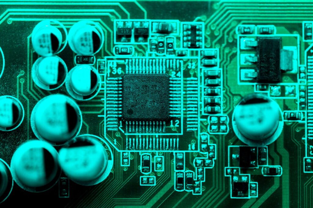
PCB Prototyping: The Physical Manifestation of the Design
After finalizing the layout, the next step is PCB prototyping. This stage involves creating a physical version of the PCB to validate the design before full-scale production. Prototyping allows designers to test the PCB’s performance and identify any issues that weren’t apparent during the schematic or layout phases.
Types of PCB Prototyping
Breadboarding:
Ideal for simple circuits, breadboarding allows designers to quickly build and test a circuit by manually connecting components. However, breadboarding may not be suitable for complex or high-frequency designs due to signal integrity issues.
Custom Fabrication:
For a more accurate representation, designers often turn to prototype fabrication services. Companies specializing in PCB manufacturing can produce custom PCBs, often within a short turnaround time, allowing for thorough testing and refinement.
Solderless Prototyping:
Another approach involves using boards with solderless connections, which can speed up testing and modifications without the need for soldering. This method is particularly useful during the early stages of prototyping, where frequent adjustments are expected.
Testing and Validation of the Prototype
Once the prototype is ready, thorough testing is essential to ensure that the PCB meets the design requirements. This process typically involves functional testing, which evaluates whether the circuit performs as expected under real-world conditions. Additional tests, such as thermal testing and signal integrity analysis, may be necessary for high-performance applications. Testing may reveal issues that require adjustments, and this iterative process—redesign, prototype, and test—is central to achieving a high-quality PCB design.
Best Practices in PCB Schematic Design and Prototyping
- Plan with DFM (Design for Manufacturability): When designing the schematic, keep manufacturing constraints in mind. This includes using components that are widely available, following standard footprints, and designing for automated assembly.
- Ensure Proper Documentation: Maintaining clear documentation, including annotated schematics, component lists, and test procedures, simplifies troubleshooting and production scaling.
- Simulate Where Possible: Many PCB design tools offer simulation capabilities, allowing designers to validate their circuits before prototyping physically.
- Follow Industry Standards: Adhere to industry standards like IPC guidelines, which ensure that designs meet rigorous quality and reliability benchmarks.
Conclusion
The journey from an initial idea to a functional PCB involves several structured phases, with PCB schematic design serving as the critical first step. This stage translates circuit ideas into a coherent visual plan, allowing for logical organization, testing, and validation before moving to PCB prototyping and ultimately production. As the demands of modern electronics evolve, designers must adopt advanced tools and adhere to best practices that facilitate error-free, scalable, and efficient design processes. Embracing these methodologies not only enhances the quality of the final product but also ensures that each circuit idea is fully realized, from conception to physical reality.