
The growing demand for smarter, smaller, and more reliable electronic products has made pcb design a cornerstone of modern engineering. Among the many tools available to designers today, Autodesk Fusion 360 stands out for integrating mechanical and electronic design into a unified environment. In this article, we explore the power and potential of pcb design in Fusion, how it compares to traditional workflows, and why it’s a game-changer for both startups and established product development teams.
What is PCB Design in Fusion?
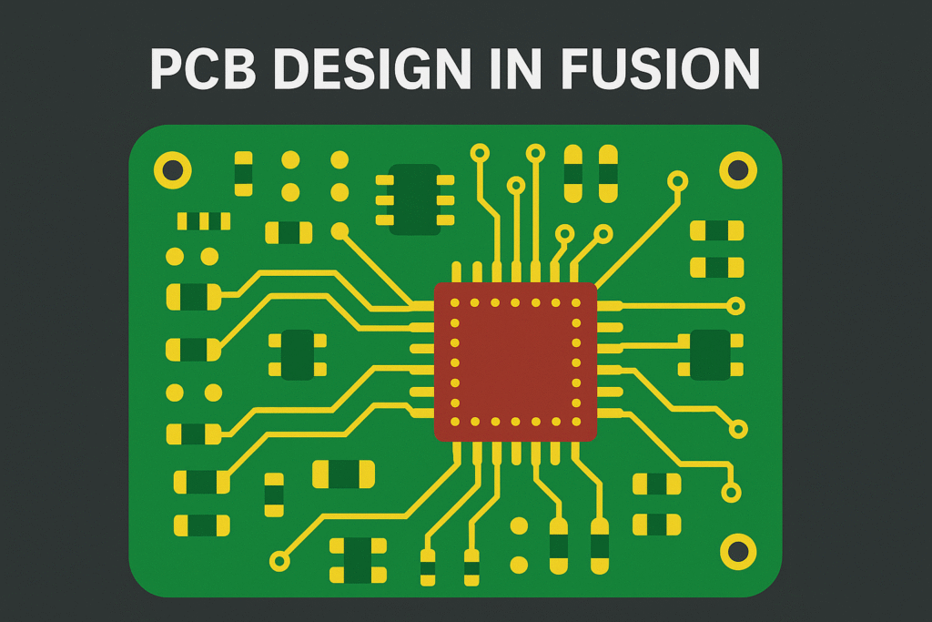
PCB design in Fusion refers to the process of creating printed circuit board layouts using Autodesk Fusion 360’s integrated electronics environment. Unlike conventional PCB tools that operate in silos, Fusion 360 bridges the gap between electrical design, mechanical integration, and manufacturing preparation. It allows engineers to go from schematic capture to 3D board layout to simulation—all within a single platform.
This fusion (no pun intended) of ECAD and MCAD workflows eliminates the usual pain points in design handoffs and ensures that your electronics perfectly align with your mechanical constraints, enclosures, and thermal profiles.
Key Features of PCB Design in Fusion
- Unified ECAD-MCAD Environment
Fusion 360 uniquely merges PCB design with 3D mechanical design. Designers can create a 2D schematic, transition to a PCB layout, and then visualize the board in a 3D assembly—all within the same file. This tight integration ensures better fit, fewer errors, and faster design cycles. - Schematic Capture and Component Libraries
Fusion 360 includes a powerful schematic editor with access to a growing library of symbols, footprints, and real-world components. You can easily add resistors, ICs, and connectors to your design and define logical relationships and net connections. - 2D PCB Layout Editor
With the layout editor, you can define board shape, place components, and route traces while managing layers, vias, and copper pours. The tool provides standard DRC (Design Rule Checking) to ensure manufacturability and signal integrity. - 3D PCB Visualization
Fusion 360’s built-in 3D PCB modeling allows designers to validate their boards in a realistic enclosure, detect collisions, and even simulate airflow or mechanical stress. This capability is especially useful in consumer products, robotics, wearables, and compact enclosures. - Version Control and Collaboration
Projects in Fusion 360 are cloud-based, allowing for real-time collaboration among distributed teams. Designers can review changes, revert to previous versions, and leave comments. Fusion’s cloud versioning is a major upgrade over traditional file-based workflows. - CAM and Manufacturing Export
Once your design is complete, Fusion 360 lets you generate Gerber files, drill files, and BOMs (Bill of Materials) for manufacturing. You can also simulate the manufacturing process for CNC drilling or milling, giving a full digital prototyping environment.
Advantages of Using Fusion 360 for PCB Design
1. End-to-End Product Development
You can go from concept to finished product—including PCB, housing, mechanical parts, and simulation—without ever leaving Fusion. This saves time and reduces dependency on multiple tools.
2. Cost-Effective and Scalable
Fusion 360 offers powerful functionality at a price point much lower than traditional PCB suites like Altium or Mentor Graphics. For startups and independent designers, this makes it an accessible option.
3. Integrated Simulation
Beyond basic electronics simulation, Fusion 360 also supports mechanical stress testing, thermal simulation, and motion analysis. This helps in identifying design bottlenecks early in the cycle.
4. Cross-Disciplinary Communication
Mechanical and electronics teams can work together in the same environment, reducing miscommunication and file translation errors between ECAD and MCAD tools.
5. Parametric Modeling
Fusion’s parametric design tools allow engineers to define constraints and relationships between components, helping in rapid iterations and design optimization.
PCB Design Workflow in Fusion
Here is a step-by-step breakdown of how PCB design in Fusion typically works:
Step 1: Create a New Electronics Design
Start by creating a new Electronics Design in Fusion. This creates a linked schematic and PCB file under a single project.
Step 2: Schematic Capture
Drag and drop components into the schematic editor. Connect the pins using the “Net” tool, and name each net for readability and future referencing. Assign footprints as needed.
Step 3: PCB Layout Setup
Define the board outline in the 2D layout space. Fusion allows you to import DXF outlines or draw the board shape manually. Set up layers and layer stacks according to your fabrication needs.
Step 4: Component Placement
Import your components from the schematic and arrange them in the PCB editor. Fusion allows you to switch between 2D and 3D views at any time, so you can instantly visualize spatial relationships.
Step 5: Routing
Use automatic or manual routing to connect your nets. Fusion includes options for via placement, differential pair routing, and trace impedance control for high-speed signals.
Step 6: Run Design Rule Checks
Once routed, run DRC to identify violations. These checks ensure that your design is within the fabrication constraints like minimum trace width, spacing, and hole sizes.
Step 7: 3D Board Preview and Mechanical Validation
Open your PCB in Fusion’s 3D environment. Add your enclosure or other mechanical components to ensure perfect alignment. Make real-time adjustments if needed.
Step 8: Manufacturing Output
Generate Gerbers, drill files, pick-and-place data, and BOM for your manufacturer. Fusion allows easy export with templates tailored for major PCB fabrication houses.
Fusion 360 vs Traditional PCB Design Tools
| Feature | Fusion 360 | Altium Designer | KiCAD | Eagle |
| ECAD-MCAD Integration | Seamless | Requires plugin | No | Limited |
| 3D Modeling | Built-in | External | No | Partial |
| Collaboration | Cloud-native | Limited | File-based | File-based |
| Simulation | Mechanical & Thermal | Electrical only | No | No |
| Licensing | Subscription (Affordable) | Expensive perpetual | Free | Free (limited) |
| Ease of Use | High | Medium | Medium | Medium |
While tools like Altium Designer offer advanced electronics simulation and multilayer signal integrity tools, Fusion 360’s real strength lies in its all-in-one workflow and ease of use, especially for integrated product design.
Use Cases for PCB Design in Fusion
- Consumer Products
Design smart wearables, game controllers, or wireless earbuds with tight mechanical-electrical integration. - Prototyping for Startups
Build prototypes quickly without buying multiple software licenses. Perfect for rapid hardware iterations. - IoT and Robotics
Create compact PCBs that fit within custom 3D-printed enclosures. Validate both electrical and mechanical interfaces. - Educational Projects
Fusion’s intuitive interface makes it ideal for teaching electronics and mechatronics in university settings. - Custom Enclosures
Design PCBs and their enclosures simultaneously to ensure perfect alignment of ports, LEDs, or mounting holes.
Tips for Better PCB Design in Fusion
- Use Named Nets: Label your signals for easier trace routing and debugging later.
- Leverage 3D Views: Always check component height and fit in the 3D view before finalizing the design.
- Create Custom Libraries: For non-standard parts, build your own footprints and 3D models for accuracy.
- Sync Schematic and PCB: Use the Fusion 360 push/pull sync to avoid mismatches between schematic and layout.
- Design with Assembly in Mind: Account for soldering clearances and mechanical stress during PCB assembly.
Future of PCB Design in Fusion
As Fusion 360 continues to evolve, Autodesk is investing in more AI-powered design automation, cloud-based manufacturing integrations, and improved library management. Soon, designers may be able to simulate EMI/EMC, heat transfer, and RF characteristics directly within Fusion. These advancements will bring professional-grade design capabilities to every desktop.
Moreover, with Fusion’s active community and Autodesk’s integration with Fusion Team and PLM tools, large-scale product lifecycle management may soon be possible for even small teams—making pcb design in Fusion not just viable, but future-ready.
Conclusion
PCB design in Fusion represents a new paradigm in electronics development—one where the lines between electrical, mechanical, and manufacturing disciplines blur for better collaboration, faster iterations, and smarter products. Whether you’re designing a complex consumer device or a simple industrial controller, Fusion 360 offers a streamlined, integrated path from idea to production. As electronics design becomes more cross-functional, tools like Fusion 360 will become indispensable in bridging the gap between design intent and manufacturing reality.