
Within electronics, the fabrication of printed circuit boards is a rather important aspect in ensuring devices work effectively and also in a reliable manner. One of the most important factors that an engineer should observe includes inductance. Understanding how inductance affects the behavior of the circuit and the design implications of it goes a long way toward enhancing performance. This article will go into detail about PCB inductance and its importance within electronic circuit design.
Understanding PCB Inductance
What is Inductance?
Inductance is the property of an electrical circuit that opposes changes in current. It occurs when a current-carrying conductor generates a magnetic field. If the current changes, the magnetic field also changes, leading to an electromotive force (EMF) that opposes the change in current. This property is fundamental in inductors, where coils of wire are often used to store energy in the magnetic field.
Inductance in Printed Circuit Boards
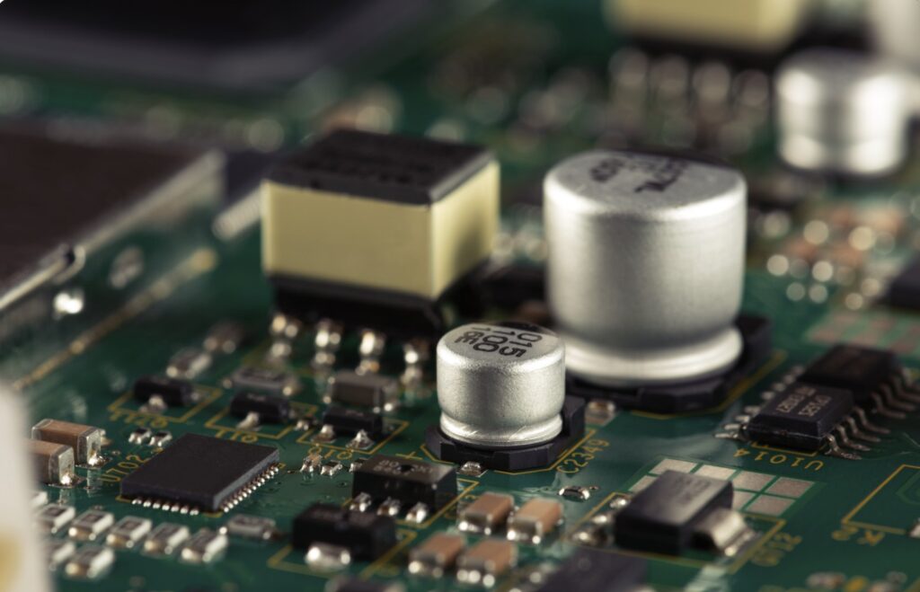
In the context of PCBs, inductance can arise from various sources, including traces, vias, and components. Each of these elements can behave like inductors, contributing to the overall inductance of the circuit. As current flows through these paths, the inductance affects how quickly the current can change, which is particularly important in high-speed digital circuits and RF designs.
The Effects of PCB Inductance on Circuit Behavior
1. Signal Integrity
One of the primary concerns with PCB inductance is its impact on signal integrity. In high-frequency applications, even small amounts of inductance can lead to significant issues. Inductive effects can cause signal distortion, ringing, and increased rise and fall times, ultimately affecting the performance of digital signals.
For instance, when a signal transitions from low to high, the inductance can slow down the current change, causing a delay in the signal’s propagation. This delay can lead to timing issues in digital circuits, making it essential to minimize inductance in critical signal paths.
2. Power Distribution
Inductance plays a crucial role in power distribution networks (PDNs) on a PCB. The distribution of power to various components requires careful consideration of inductance to ensure stable voltage levels across the board. High inductance in power traces can lead to voltage drops and fluctuations, resulting in insufficient power delivery to components.
Transient loads, such as those found in microcontrollers and processors, can exacerbate these issues, causing voltage sag or spikes. Therefore, minimizing PCB inductance is critical to maintaining stable power delivery and avoiding performance degradation.
3. EMI and Crosstalk
Electromagnetic interference (EMI) and crosstalk are significant concerns in PCB design, particularly for high-speed circuits. PCB inductance contributes to the coupling of electromagnetic fields between traces, which can lead to unwanted noise and signal degradation.
Higher inductance paths can act as antennas, radiating signals that interfere with nearby circuits. Additionally, inductance can enhance crosstalk between adjacent traces, where the changing magnetic fields of one trace induce voltages in neighboring traces. To mitigate these effects, designers must carefully route traces and consider the inductive properties of each element on the PCB.
PCB Design Considerations to Minimize Inductance
1. Trace Width and Length
One of the most straightforward ways to reduce PCB inductance is by optimizing trace width and length. Wider traces have lower resistance and inductance, allowing for better current handling and signal integrity. However, increasing the width may also reduce the available space on the PCB, so designers must find a balance based on the specific application.
Shortening trace lengths can also reduce inductance, as longer traces have more resistance and inductance. Designers should aim to minimize the distance between components to reduce the length of high-frequency signal paths.
2. Via Design
Vias are often necessary for connecting different layers of a PCB, but they also introduce additional inductance. To minimize this impact, engineers can use larger vias, multiple vias in parallel, or blind/buried vias that reduce the overall inductive loop area. Additionally, minimizing the number of vias in critical signal paths can help maintain signal integrity.
3. Ground Planes
Incorporating solid ground planes into PCB designs significantly reduces inductance. A ground plane provides a low-inductance return path for current, helping to stabilize signals and minimize EMI. Ground planes also help with thermal management, providing a way to dissipate heat generated by components.
4. Component Placement
Strategic placement of components can also help reduce PCB inductance. Designers should position high-frequency components close to each other to minimize trace lengths. Additionally, decoupling capacitors should be placed as close as possible to the power pins of ICs to reduce inductive effects in power delivery.
5. Layer Stackup
The arrangement of layers in a PCB can significantly affect inductance. Multi-layer PCBs often have dedicated power and ground layers that can help reduce inductance. By carefully designing the layer stackup and ensuring proper spacing between layers, engineers can minimize the inductive coupling between signal layers and ground or power layers.
Testing and Simulation of PCB Inductance
1. Simulation Tools
Before manufacturing a PCB, engineers often rely on simulation tools to analyze inductance and its effects on circuit behavior. Software like SPICE, ANSYS, and HyperLynx can model inductive effects, helping designers visualize how changes in trace routing or component placement will impact performance.
2. Prototype Testing
Once a PCB design is finalized, it is crucial to test prototypes to validate the inductance and overall performance of the circuit. Engineers can use oscilloscopes and network analyzers to measure signal integrity, voltage levels, and response times. These tests help identify any issues related to PCB inductance and allow for adjustments before final production.
Conclusion
PCB inductance is a critical factor that significantly influences circuit behavior and design. Understanding how inductance affects signal integrity, power distribution, and EMI can help engineers create more reliable and high-performing electronic devices. By considering design strategies to minimize inductance, such as optimizing trace width and length, utilizing ground planes, and strategically placing components, engineers can enhance the performance of their PCBs.
In an era of ever-increasing demand for high-speed and efficient electronic devices, a deep understanding of PCB inductance is essential. As technology continues to evolve, the principles of inductance will remain a cornerstone of effective PCB design, ensuring that electronic circuits can meet the challenges of modern applications.
By prioritizing inductance in the design process, engineers can create PCBs that not only function effectively but also stand the test of time in a rapidly changing technological landscape. Whether designing for consumer electronics, automotive applications, or advanced communication systems, the importance of managing PCB inductance cannot be overstated