
In the dynamic landscape of electronics, transforming an idea into a completed product typically encompasses numerous stages of refinement and testing. One of the most crucial of these stages is PCB prototyping, which plays a vital role in ensuring that electronic devices function reliably and adhere to specified requirements. This article delves into the importance of PCB prototyping within the realms of PCB design and manufacturing, as well as the diverse methodologies and technologies that make it an essential component of the development process.
Understanding PCB Prototyping
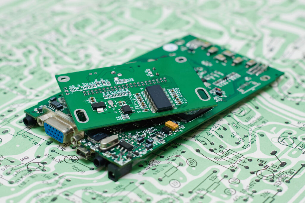
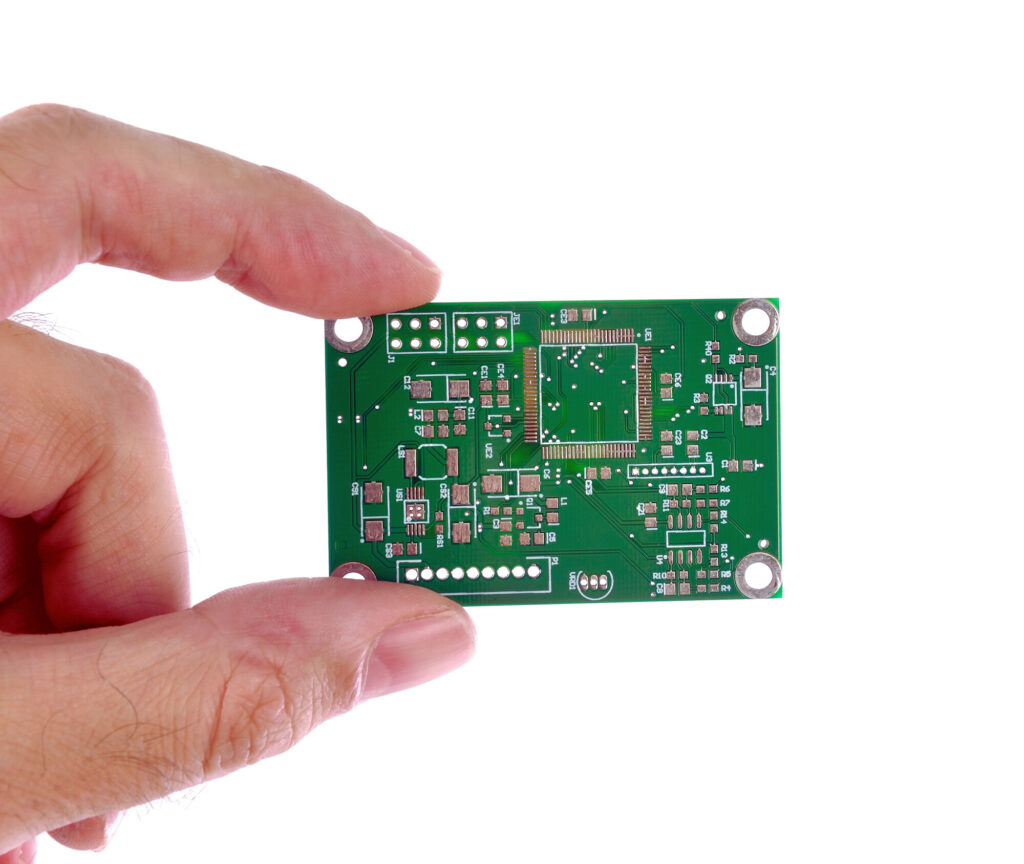
PCB prototyping refers to the process of creating a preliminary version of a printed circuit board before full-scale production. This prototype is instrumental in validating the design, functionality, and manufacturability of the final product. Prototyping can range from simple breadboards or single-layer boards to complex multilayer PCBs, depending on the requirements of the design.
The Importance of PCB Prototyping
1. Design Validation
Before full-scale production, it’s crucial to test and validate the design of the PCB. Prototyping allows engineers to check for design flaws, component placements, and the overall functionality of the circuit. By identifying problems during the prototyping phase, developers can avoid expensive changes during the manufacturing phase.
2. Cost Efficiency
Prototyping can significantly lower costs in the long run. Although there are upfront costs associated with creating a prototype, finding issues early can prevent costly redesigns, product recalls, and wasted materials during mass production.
3. Accelerating Time to Market
Market competition in electronics is fierce. Prototyping helps accelerate the development cycle by enabling faster iterations and testing. This agility allows companies to reduce their time to market, a crucial factor in leveraging competitive advantages.
4. Enhanced Communication
Prototypes serve as tangible representations of the concept, facilitating better communication between designers, engineers, and stakeholders. Having a physical prototype makes it easier to discuss features, improvements, and client expectations.
The PCB Design Process
Effective PCB prototyping begins with a well-defined design process. This process includes several key stages:
1. Schematic Design
The design phase starts with creating a schematic diagram that outlines the electrical connections between components. This representation is crucial for visualizing how each component will interact within the circuit.
2. Layout Design
Once the schematic is finalized, the next step is layout design. This involves arranging the components on the PCB and routing the connections. During this phase, design rules must be adhered to, including trace width, spacing, and layer stacking.
3. Simulation and Analysis
Before fabricating the PCB, engineers often use simulation tools to analyze the circuit’s behavior under different scenarios. Parameters such as current flow, thermal performance, and noise can be studied. Such analysis is essential to ensure that the design will operate correctly in real-world conditions.
4. Creating the Gerber Files
After finalizing the layout, engineers generate Gerber files, which are standard files used in PCB manufacturing. These files provide the necessary information for fabricators to produce the physical circuit board.
PCB Manufacturing Process
PCB manufacturing follows the design and prototyping phases. Understanding this process is vital for realizing the importance of prototyping:
1. Materials Selection
Choosing the right materials is essential. PCBs are typically made from a combination of copper and different substrates such as FR-4 or flexible material. The selected materials influence the board’s performance, durability, and thermal management.
2. Fabrication Techniques
Various techniques are employed in PCB manufacturing, including etching, plating, drilling, and lamination. The choice of technique can depend on the complexity of the design, the number of layers, and the desired finish.
3. Assembly
After manufacturing the bare PCB, the next step is assembly. This involves soldering components onto the board, which can either be done manually or through automated processes like Surface Mount Technology (SMT).
4. Testing and Quality Control
Quality assurance is critical in ensuring the reliability of PCBs. Testing methods such as Automated Optical Inspection (AOI) or X-ray inspection are employed to detect defects. This stage can reveal important insights that inform future designs, enhancing the overall process.
Methods of PCB Prototyping
There are various methods for PCB prototyping, each with its own set of advantages and limitations. Here are some of the most commonly used techniques:
1. Breadboarding
This is a non-permanent way to create a prototype circuit. Engineers use a breadboard to test electronic components by inserting wires and components into a grid. While this is an excellent method for initial testing, it is not suitable for final prototypes that require specific layouts and connections.
2. Rapid Prototyping
Rapid prototyping involves various technologies such as 3D printing and CNC machining to create physical models quickly. Technologies like additive manufacturing may be applied to design customized PCBs more effectively.
3. Low-Volume PCB Manufacturing
For those needing a more permanent prototype, low-volume manufacturing services allow engineers to order a small batch of PCBs. This method provides more accurate results compared to breadboarding while maintaining a focus on cost-effectiveness.
4. Solderless Prototyping Boards
These boards allow components to be inserted without soldering, enabling quick changes and modifications. These are particularly useful in educational and testing environments.
Challenges in PCB Prototyping
While PCB prototyping is invaluable, it is not without its challenges:
1. Complexity of Designs
As designs become more intricate, prototyping can be more challenging. Multilayer PCBs or designs requiring advanced components may necessitate specialized services.
2. Time Constraints
While prototyping is meant to enhance efficiency, tight development timelines can pose issues. Striking a balance between thorough testing and meeting deadlines can be difficult.
3. Quality Assurance
Prototypes may not always reflect the quality of mass-manufactured boards. Ensuring that prototypes are tested rigorously can help identify flaws that may not present themselves until a later stage.
Future Trends in PCB Prototyping
The landscape of PCB prototyping is continually evolving, influenced by technological advancements and industry demands:
1. Increased Use of Automation
Automation in PCB production and prototyping is on the rise, enabling faster cycles and consistent quality. Automated assembly and inspection processes reduce human error and enhance efficiency.
2. IoT Integration
As the Internet of Things (IoT) expands, the demand for smart and interconnected devices rises. This necessitates more sophisticated PCB designs and consequently more refined prototyping processes.
3. Sustainability Practices
Environmental concerns are prompting manufacturers and designers to adopt eco-friendly materials and processes in PCB prototyping. Recycled materials and reduced waste techniques are becoming more prevalent.
4. Advanced Simulation Tools
Emerging simulation software that embodies Artificial Intelligence (AI) and Machine Learning (ML) enhances the design validation processes, allowing engineers to rapidly iterate and visualize PCB performance.
Conclusion
Prototyping PCBs is a critical phase in the development of reliable electronic devices. It allows engineers to validate their designs, enhance user functionality, and discover potential flaws before committing to mass production. By investing time and resources into effective prototyping methods — including those from Arshon Technology teams can shorten development cycles, reduce costs, and ultimately create higher-quality products that meet user needs and industry standards. As technology continues to advance, the methods and practices surrounding PCB prototyping will likely evolve, paving the way for innovations in the electronics industry.