
In the fast-moving world of wireless technology, the need for efficient and reliable RF circuit design for wireless applications is more important than ever. From smartphones and IoT sensors to satellite communication systems and industrial wireless modules, radio frequency circuits lie at the heart of every modern wireless device. This type of design demands deep understanding of analog signal behavior, electromagnetic theory, and high-frequency PCB layout techniques. At the core of all these requirements is precise pcb design, which plays a vital role in shaping RF signal integrity and performance.
Designing RF circuits is different from low-frequency or purely digital electronics. In the RF domain, every component, trace, pad, and connector can act as a passive device, affecting impedance, resonance, and coupling. The task of the designer is to balance gain, bandwidth, noise, stability, and efficiency across a targeted frequency range. This article offers a complete technical view into how RF circuits are engineered for wireless applications, the types of components involved, and the best practices that lead to optimized performance and compliance with regulations.
Understanding the Basics of RF Design
Radio frequency (RF) refers to alternating current signals that oscillate at frequencies between 3 kHz and 300 GHz. In wireless systems, RF circuits are responsible for transmitting and receiving these high-frequency signals through antennas. The circuit elements that process these signals must be designed to work in this frequency band while maintaining signal fidelity and minimizing losses.
Key Parameters in RF Circuit Design
- Frequency: The target operating frequency determines component choices and trace dimensions.
- Impedance: Most RF systems operate at 50 ohms impedance. Matching the impedance across the signal path is critical for reducing reflection.
- Return Loss and VSWR: These parameters measure how much signal is reflected due to impedance mismatches.
- Noise Figure (NF): Determines how much noise is introduced by the circuit. Lower NF is ideal for receivers.
- Gain and Linearity: For amplifiers, the gain must be stable across the band while maintaining low distortion.
- Bandwidth: Defines the frequency range over which the circuit must function effectively.
Typical RF Circuit Blocks
- Low-Noise Amplifier (LNA): Placed close to the antenna in receivers to boost weak signals while minimizing noise.
- Power Amplifier (PA): Drives the antenna in transmitters and must operate efficiently while maintaining linearity.
- Mixers: Used in frequency translation to convert RF signals to intermediate frequency (IF) or baseband.
- Oscillators and PLLs: Provide stable frequency references used in tuning and modulation.
- Filters: Remove unwanted frequency components such as harmonics or adjacent channel noise.
- Attenuators and Switches: Manage power levels and routing in transmit/receive chains.
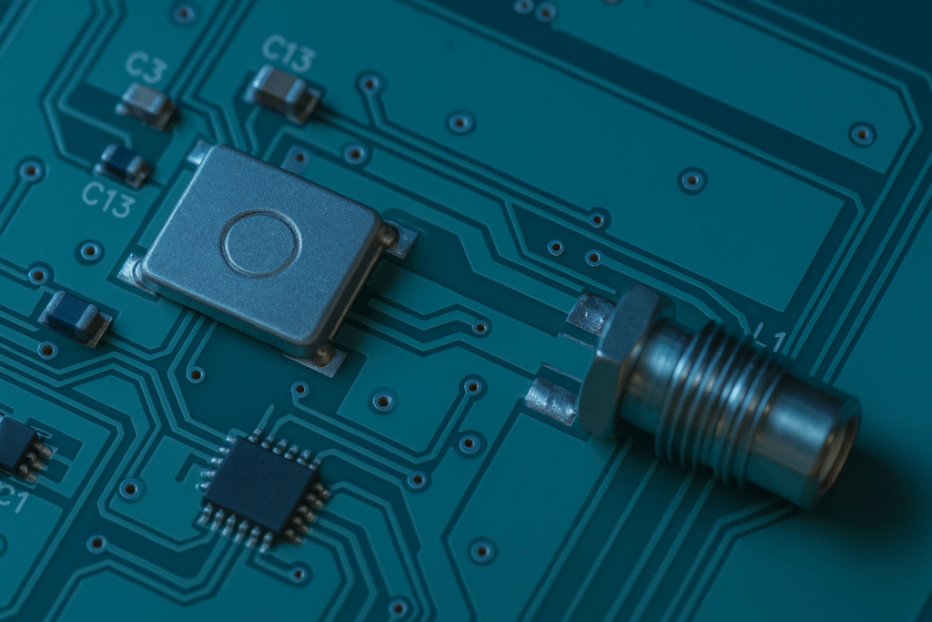
Pcb Design Considerations for RF Circuits
The layout of an RF printed circuit board plays a major role in how the circuit performs. Unlike digital designs where timing and logic states are paramount, RF design must account for transmission line effects, radiation, parasitic capacitance, and dielectric losses.
1. Controlled Impedance Traces
- Microstrip and stripline configurations are used to control impedance.
- Trace width, substrate thickness, and dielectric constant must be calculated to achieve 50 ohm impedance.
- Tools like impedance calculators or field solvers can guide the layout.
2. Grounding and Shielding
- A continuous ground plane under RF traces helps control return paths and reduces EMI.
- Via stitching along ground edges enhances shielding and minimizes coupling.
- Metal enclosures or shield cans are often placed over sensitive RF sections.
3. Trace Routing
- Keep RF traces as short and direct as possible to minimize loss.
- Avoid sharp corners—use mitered or curved bends to reduce reflections.
- Isolate digital and RF sections to prevent interference.
4. Decoupling and Bypassing
- Place decoupling capacitors close to RF IC power pins to suppress high-frequency noise.
- Use a hierarchy of values (e.g., 0.1 µF, 10 nF, 1 nF) to cover different frequency ranges.
5. Component Placement
- Place LNA close to the antenna to reduce cable losses.
- Keep high-power amplifiers away from sensitive receivers.
- Minimize parasitic inductance and capacitance by using compact pad layouts.
RF Simulation and Modeling
Before fabrication, RF circuits should be simulated to verify performance. Simulation tools provide visibility into S-parameters, noise, impedance, and matching.
- Schematic Simulation: Software like Keysight ADS, NI AWR, or LTspice is used for basic circuit-level simulation.
- Electromagnetic Simulation: 3D field solvers (e.g., Ansys HFSS) model PCB traces, antennas, and enclosures.
- Harmonic Balance and Noise Analysis: Assess nonlinear effects and noise contributions in amplifiers and mixers.
Matching Networks and Impedance Tuning
An essential part of RF design is building matching networks to achieve maximum power transfer. When impedance between source and load is mismatched, significant signal loss can occur.
- LC Matching: Use capacitors and inductors in L-type, Pi-type, or T-type configurations.
- Smith Chart: A graphical tool used for solving impedance transformation and visualizing reflection coefficients.
- Automatic Matching: Some RF ICs feature built-in tuning algorithms for adjusting impedance in real time.
Antenna Interface and Layout
The connection between the RF circuit and antenna requires careful design to maintain performance across the frequency band.
- Antenna Matching: Use S-parameter measurements and matching networks to achieve minimal return loss at the target frequency.
- Baluns and Feedlines: Convert between differential and single-ended signals while maintaining impedance.
- Keepouts: Avoid placing copper or ground near antennas unless it’s part of the intended design.
Noise Management in RF Receivers
Low noise is critical in receivers. Noise comes from thermal sources, power supply ripple, and other active components. Effective design minimizes noise figure and improves receiver sensitivity.
- Isolate analog and digital grounds to avoid cross-interference.
- Use linear regulators instead of switching ones where ripple is unacceptable.
- Low-pass filters on power inputs block conducted noise.
Power Amplifier Design Tips
In transmitter sections, the power amplifier determines output strength, efficiency, and regulatory compliance.
- Class A, B, AB, and C amplifiers offer trade-offs in linearity and efficiency.
- Efficiency is maximized using envelope tracking or Doherty architectures.
- Thermal management is vital—use heatsinks, thermal vias, and copper planes under high-power devices.
RF Circuit Testing and Validation
After building the circuit, real-world measurements validate whether performance targets are met.
- Vector Network Analyzer (VNA): Measures gain, loss, VSWR, and S-parameters.
- Spectrum Analyzer: Evaluates output power, harmonics, spurious signals.
- Oscilloscope: Captures waveform characteristics like modulation and distortion.
- Anechoic Chamber: Used for over-the-air testing of antennas and RF performance.
Regulatory Compliance and Certification
RF devices must comply with international standards to prevent interference and ensure safety.
- FCC (USA), CE (Europe), IC (Canada): Regulate emission limits and frequencies.
- ETSI and ITU: Define protocol-specific behaviors and frequency plans.
- Pre-certification testing helps identify issues before formal testing begins.
Common Applications of RF Circuit Design
- Wi-Fi Routers: Use multiple antennas, filters, and dual-band circuits.
- Bluetooth Modules: Require compact, low-power designs with integrated matching.
- Cellular Devices: Feature power amplifiers, duplexers, and multi-band support.
- LoRa and Zigbee: Use sub-GHz frequencies for low-power wide-area networks (LPWANs).
- Satellite Terminals: Use high-frequency Ku or Ka band circuits with low noise and high linearity.
- Radar Systems: Employ frequency modulation, power gain control, and phase-matched paths.
Future Trends in RF Design
- 5G mmWave: Pushes RF design into 24 GHz and beyond, requiring special substrates and miniaturized passive components.
- AI-Enabled Radios: Use machine learning to adapt power, frequency, and gain in real-time.
- Software-Defined Radios (SDRs): Allow hardware flexibility for multiple protocols and frequencies.
- Quantum and Terahertz RF: Pushing boundaries in security, sensing, and ultra-high-speed communication.
Conclusion
The design of RF circuits is both art and science. It demands accuracy, experience, and a strong grasp of electromagnetic behavior. A successful RF circuit design for wireless applications combines simulation, precise pcb layout, careful component selection, and rigorous testing. By understanding the core elements of RF systems—amplifiers, filters, oscillators, matching networks, and antennas—engineers can build high-performance wireless products that meet modern standards of speed, efficiency, and reliability.
Whether you’re working on consumer IoT or mission-critical communications, starting with a clean and thoughtful pcb design sets the foundation for RF performance and regulatory success.