
Signal integrity in high-frequency PCB design is one of the most critical aspects engineers need to address to achieve optimal performance in modern electronics. Whether you are working on RF systems, high-speed digital circuits, or advanced communication devices, ensuring clean, reliable signals is at the core of successful pcb design. As frequencies increase, maintaining signal integrity becomes more challenging, requiring precision, careful planning, and specialized tools. This article provides an in-depth look at signal integrity in high-frequency PCB design, practical tips for achieving robust results, common challenges, and tools that help ensure success.
Signal Integrity in PCB Design
Signal integrity refers to the quality and reliability of the electrical signals as they travel through a PCB. In low-frequency designs, signal degradation might not significantly impact functionality, but in high-frequency applications, even small impairments can lead to data loss, timing errors, and electromagnetic interference (EMI). Key factors influencing signal integrity in PCB design include impedance matching, trace geometry, dielectric materials, termination schemes, and the interaction between signals and power delivery networks.
The demand for faster data rates and higher bandwidths in devices such as 5G systems, automotive radar, aerospace communication equipment, and high-speed storage solutions means engineers must give signal integrity top priority. A well-thought-out pcb design can minimize losses, reflections, and crosstalk while preserving signal fidelity even at gigahertz frequencies.
Tips for High-Frequency PCB Design
When working on high-frequency designs, applying specific strategies can greatly reduce the risk of signal integrity issues. Here are essential tips:
1. Control impedance: Every high-speed trace should have a controlled impedance, typically 50 ohms for single-ended lines or 100 ohms for differential pairs. This requires precise trace width, spacing, and reference plane planning.
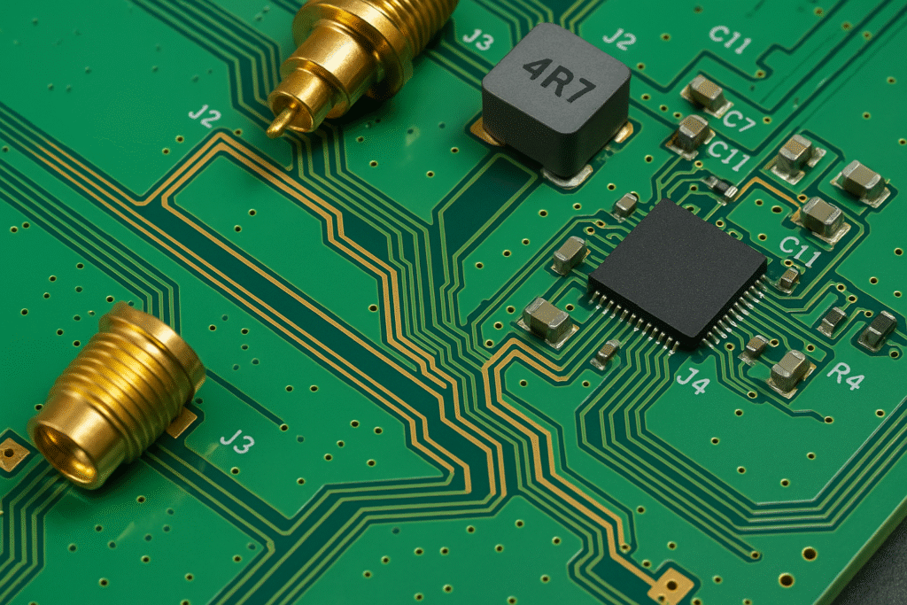
2. Minimize via usage: Vias introduce inductance and capacitance that can degrade signal integrity, especially at higher frequencies. Minimize their use, and if unavoidable, choose backdrilled or blind/buried vias.
3. Use ground planes: A continuous ground plane under high-speed traces provides a stable return path, reducing loop area and EMI. Avoid splitting ground planes under critical signals.
4. Keep trace lengths matched: Differential pairs must have equal lengths to prevent timing skews. Use serpentine routing only when necessary and avoid excessive meandering.
5. Proper layer stack-up: A good stack-up reduces crosstalk and EMI while helping maintain impedance. A typical high-frequency stack-up alternates signal layers with power or ground planes.
6. Terminate signals correctly: Use appropriate termination techniques like series termination or Thevenin termination to prevent reflections at high speeds.
7. Shorter stub lengths: If stubs are part of the design (e.g., for test points), keep them as short as possible to reduce signal reflections and resonances.
8. Select high-quality materials: Low-loss dielectric materials such as Rogers, Taconic, or Megtron provide lower insertion loss at high frequencies than standard FR-4.
Maintaining Signal Integrity
Maintaining signal integrity starts from schematic design and carries through to layout and manufacturing. Best practices include:
- Careful component placement to minimize trace lengths and crossings.
- Isolating high-speed and low-speed signals to prevent interference.
- Paying attention to power integrity, as poor power delivery can indirectly affect signal quality through voltage noise and ground bounce.
- Shielding sensitive areas or signals when external interference is a concern.
- Running pre-layout and post-layout simulations to validate signal performance before production.
In high-frequency PCB design, it is important to treat power distribution networks (PDNs) with the same care as signal traces. Decoupling capacitors must be placed close to IC power pins, and power planes must be solid with adequate copper weight.
Challenges in High-Frequency PCB Design
Designers face several challenges when dealing with high-speed and RF boards:
Crosstalk: When signal traces run parallel for extended distances, energy can couple from one trace to another, leading to unwanted noise. Keeping spacing at least 3x the trace width between adjacent signals helps minimize this effect.
Reflections: Impedance mismatches at any point along a trace (due to discontinuities, stubs, connectors) can reflect part of the signal back towards the source. This degrades signal quality and may violate timing requirements.
Attenuation: High frequencies experience greater loss over distance due to skin effect and dielectric loss. This limits the maximum length of traces without amplification or equalization.
EMI: High-frequency signals radiate more readily, posing compliance challenges. A careful combination of shielding, ground planes, and controlled impedance is required to meet EMC regulations.
Manufacturing variations: Small changes in etching, plating, or material properties can alter impedance and affect performance. It is important to work with reliable PCB manufacturers familiar with high-speed requirements.
Tools for Signal Integrity Analysis
Modern high-frequency PCB design is supported by advanced tools that help simulate and validate signal integrity before the first prototype is built.
SI simulation software: Tools like Keysight ADS, Ansys HFSS, HyperLynx, and Cadence Sigrity allow designers to model transmission lines, simulate eye diagrams, and predict EMI performance.
3D EM field solvers: These tools help model complex structures such as connectors, packages, and via transitions with high accuracy.
TDR (Time Domain Reflectometry): TDR equipment is used to analyze physical boards, detecting impedance discontinuities and reflections on actual prototypes.
SPICE-based simulation: Useful for analyzing the interaction of circuits and transmission lines, especially in mixed-signal designs.
Incorporating these tools into the design workflow helps identify potential problems early, saving cost and time in development cycles.
Conclusion
Signal integrity in high-frequency PCB design requires a balance of science, experience, and meticulous attention to detail. As electronic systems push into higher data rates and more demanding applications, addressing signal integrity issues becomes more critical than ever. By applying good design practices, using appropriate materials, leveraging simulation tools, and partnering with experienced manufacturers, engineers can deliver reliable, high-performance designs that meet modern requirements.