
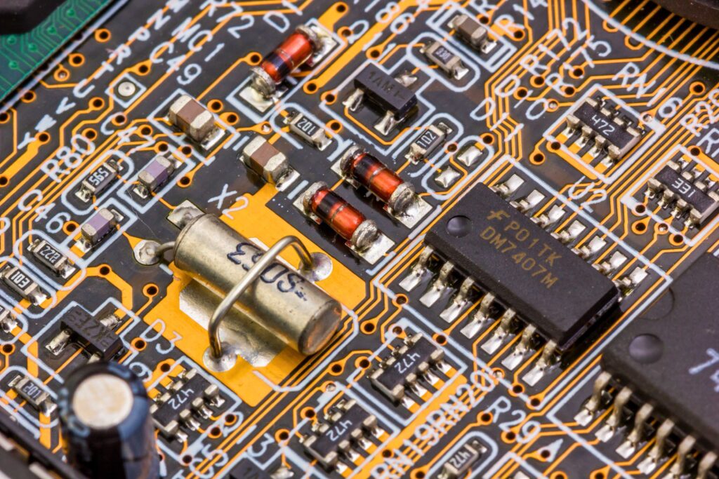
Circuit board layout design is a critical aspect of developing electronic devices. It involves arranging the components on a printed circuit board (PCB) and designing the pathways for electrical connections. This guide will delve into 25 essential keywords related to circuit board layout design, providing a detailed explanation for each.
1. Circuit Board Layout Design

Circuit board layout design is the process of arranging electronic components and routing electrical connections on a PCB. This process transforms a schematic diagram into a physical board that can be manufactured and used in electronic devices.
Key Steps
1. Schematic Capture: Creating a detailed diagram of the electronic circuit.
2. Component Placement: Strategically placing components on the PCB to optimize performance and manufacturability.
3. Routing: Designing the electrical connections between components.
4. Design Rule Checking (DRC): Ensuring the design adheres to manufacturing constraints and industry standards.
5. Simulation and Testing: Verifying the design through simulations and physical prototypes.
Importance
Circuit board layout design is crucial for the functionality and reliability of electronic devices. A well-designed layout ensures efficient signal transmission, minimizes interference, and facilitates heat dissipation.
Applications
– Consumer Electronics: Smartphones, tablets, laptops.
– Automotive Electronics: Engine control units, infotainment systems.
– Medical Devices: Diagnostic equipment, wearable health monitors.
– Industrial Equipment: Control systems, robotics.

2. PCB Layout Services
PCB layout services involve professional design services provided by experts to create efficient and reliable PCB layouts. These services ensure that the design is optimized for performance, manufacturability, and cost-effectiveness.
Key Aspects
– Expertise: Professional designers with extensive experience in PCB layout design.
– Advanced Tools: Utilization of the latest design software and tools.
– Customization: Tailored designs to meet specific project requirements.
– Quality Assurance: Thorough testing and validation to ensure design integrity.
Benefits
– Time Efficiency: Faster design process with professional services.
– Cost Savings: Avoiding costly mistakes through expert design.
– Enhanced Performance: Optimized designs for better performance and reliability.
Applications
– Prototyping: Developing prototypes for testing and validation.
– Mass Production: Designing PCBs for large-scale manufacturing.
– Custom Projects: Specialized designs for unique applications.
3. High-Speed Circuit Board Layout
High-speed circuit board layout focuses on designing PCBs that handle high-frequency signals. These designs require special considerations to maintain signal integrity and prevent issues such as electromagnetic interference (EMI).
Design Considerations
– Signal Integrity: Ensuring clean signal transmission without distortion.
– Impedance Matching: Matching the impedance of transmission lines to prevent signal reflections.
– Controlled Impedance: Designing traces with precise impedance control.
– Minimizing Crosstalk: Reducing interference between adjacent traces.
Importance
High-speed PCB layouts are essential for applications such as telecommunications, data centers, and high-performance computing. Ensuring signal integrity at high frequencies is critical for the reliable operation of these systems.
Applications
– Networking Equipment: Routers, switches, servers.
– Telecommunications: Mobile base stations, satellite communications.
– High-Performance Computing: Supercomputers, data processing units.
– Consumer Electronics: High-speed data transfer devices.
4. Multilayer PCB Layout
Multilayer PCB layout involves designing PCBs with multiple layers of conductive material, allowing for more complex and compact designs. These PCBs are used in advanced electronic devices where space is limited.
Key Features
– Increased Component Density: More components can be placed on a smaller board.
– Improved Signal Integrity: Reduced signal interference with dedicated ground and power planes.
– Enhanced Thermal Management: Better heat dissipation through multiple layers.
– Complex Routing: Easier routing of complex circuits with multiple layers.
Design Process
– Layer Stack-Up: Designing the arrangement of layers in the PCB.
– Power and Ground Planes: Allocating dedicated layers for power and ground connections.
– Routing Strategy: Planning the routing of signals across different layers.
– Thermal Analysis: Ensuring adequate heat dissipation.
Applications
– Advanced Electronics: Smartphones, tablets, laptops.
– Telecommunications: Networking equipment, base stations.
– Medical Devices: Diagnostic equipment, wearable technology.
– Automotive Electronics: Engine control units, infotainment systems.
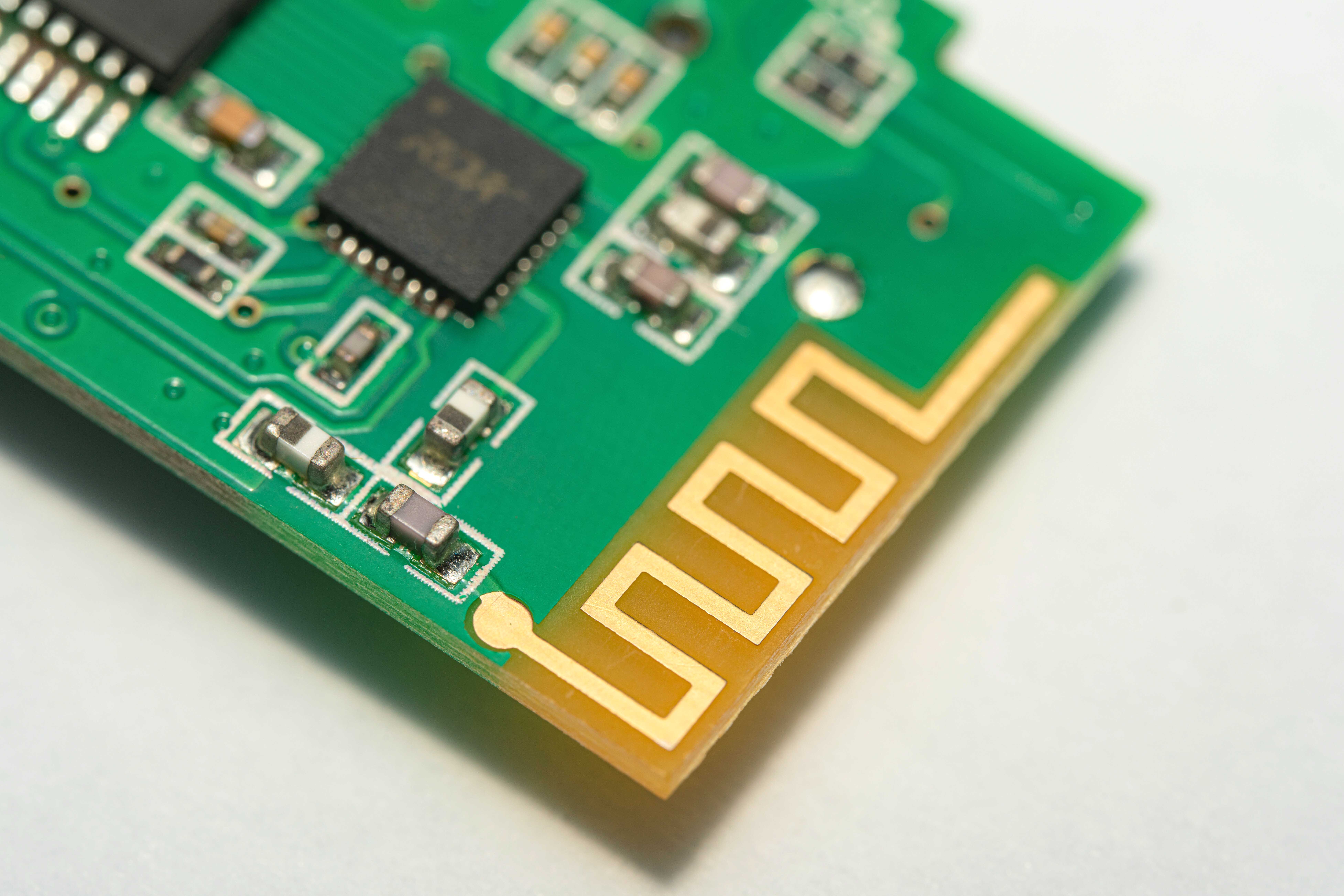
5. RF Circuit Board Layout
RF (Radio Frequency) circuit board layout focuses on designing PCBs for circuits that operate at high frequencies. These designs require special considerations to ensure efficient transmission of radio signals.
Design Considerations
– Signal Integrity: Ensuring minimal signal loss and distortion.
– Impedance Control: Maintaining precise impedance for RF signals.
– Shielding: Using shielding techniques to prevent EMI.
– Component Placement: Strategic placement to minimize interference and signal loss.
Importance
RF PCB layouts are essential for wireless communication systems, including mobile phones, Wi-Fi devices, and satellite communications. Ensuring efficient and reliable RF signal transmission is critical for these applications.
Applications
– Mobile Communications: Smartphones, tablets.
– Wi-Fi Devices: Routers, access points.
– Satellite Communications: Ground stations, satellite transceivers.
– IoT Devices: Wireless sensors, smart home devices.
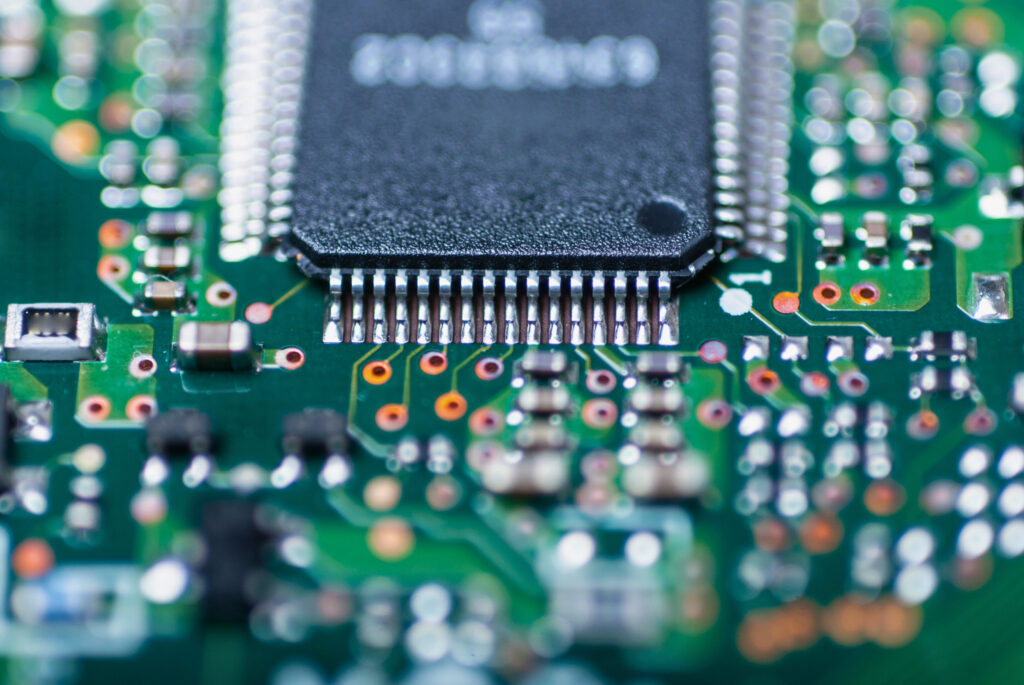
6. PCB Component Placement
PCB component placement involves strategically arranging electronic components on the PCB to optimize performance, manufacturability, and reliability. Proper component placement is crucial for efficient circuit operation and minimizing interference.
Key Considerations
– Signal Flow: Arranging components to ensure efficient signal flow.
– Thermal Management: Placing heat-generating components to facilitate heat dissipation.
– Minimizing Crosstalk: Reducing interference between adjacent components.
– Ease of Assembly: Ensuring components are placed for easy manufacturing and assembly.
Importance
Proper component placement is essential for the functionality and reliability of the PCB. It impacts signal integrity, thermal performance, and the overall manufacturability of the board.
Applications
– High-Speed Circuits: Ensuring signal integrity at high frequencies.
– Power Electronics: Efficient heat dissipation and power management.
– Compact Designs: Maximizing space utilization in small form-factor devices.
– Complex Circuits: Simplifying routing in multilayer PCBs.
7. PCB Routing Techniques
PCB routing techniques involve designing the electrical connections between components on the PCB. Effective routing ensures signal integrity, minimizes interference, and facilitates manufacturability.
Key Techniques
– Trace Width and Spacing: Ensuring appropriate width and spacing for signal and power traces.
– Differential Pair Routing: Routing pairs of traces with controlled impedance for high-speed signals.
– Via Usage: Using vias to connect different layers of the PCB.
– Power and Ground Planes: Using dedicated planes for power and ground connections.
Importance
Effective PCB routing is crucial for the performance and reliability of the electronic device. Proper routing minimizes signal loss, interference, and ensures efficient power distribution.
Applications
– High-Speed Circuits: Ensuring signal integrity for high-frequency signals.
– Power Electronics: Efficient routing of power traces.
– Multilayer PCBs: Complex routing across multiple layers.
– Compact Designs: Optimizing space utilization in small form-factor devices.
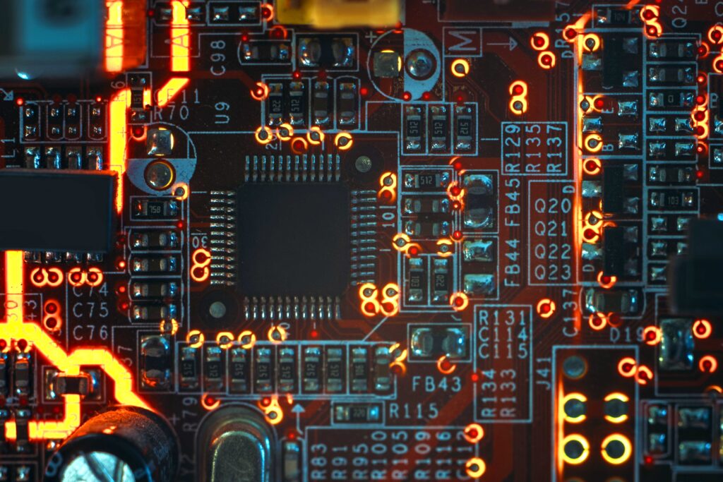
8. Signal Integrity in PCB Design
Signal integrity in PCB design involves ensuring that electrical signals are transmitted without distortion, loss, or interference. Maintaining signal integrity is critical for the reliable operation of electronic devices.
Key Factors
– Impedance Matching: Ensuring the impedance of transmission lines matches the source and load to prevent reflections.
– Crosstalk: Minimizing interference between adjacent signal traces.
– Grounding: Providing a stable ground reference to reduce noise and interference.
– Trace Layout: Designing traces to maintain signal integrity, especially for high-speed signals.
Importance
Maintaining signal integrity is essential for the proper functioning of high-speed and high-frequency circuits. Poor signal integrity can lead to data corruption, signal loss, and malfunction of the electronic device.
Applications
– High-Speed Data Transfer: Ensuring reliable data transmission in networking equipment.
– Telecommunications: Maintaining signal quality in communication devices.
– Consumer Electronics: Reliable operation of smartphones, tablets, and laptops.
– Automotive Electronics: Ensuring signal integrity in advanced driver-assistance systems (ADAS).
9. PCB Thermal Management
PCB thermal management involves designing PCBs to effectively dissipate heat generated by electronic components. Proper thermal management is crucial for the reliability and longevity of electronic devices.
Key Techniques
– Heat Sinks: Using heat sinks to dissipate heat from high-power components.
– Thermal Vias: Adding vias to transfer heat between layers of the PCB.
– Copper Planes: Using large copper planes to spread heat.
– Component Placement: Placing heat-generating components to facilitate heat dissipation.
Importance
Effective thermal management is essential to prevent overheating, which can lead to component failure and reduced lifespan of the electronic device. Proper thermal design ensures reliable operation and performance.
Applications
– Power Electronics: Efficient heat dissipation in power supplies and converters.
– High-Power LED Lighting: Managing heat in LED lighting systems.
– Computing Devices: Cooling in laptops, desktops, and servers.
– Automotive Electronics: Thermal management in engine control units and infotainment systems.
10. EMI/EMC Considerations in PCB Design
EMI (Electromagnetic Interference) and EMC (Electromagnetic Compatibility) considerations in PCB design involve designing PCBs to minimize interference and ensure compatibility with other electronic devices.
Key Techniques
– Shielding: Using shielding to block EMI from external sources.
– Grounding: Providing a stable ground to reduce noise and interference.
– Filtering: Adding filters to suppress unwanted signals.
– Trace Layout: Designing traces to minimize EMI and ensure EMC.
Importance
EMI and EMC considerations are critical for the reliable operation of electronic devices in environments with various electromagnetic sources. Ensuring EMC compliance is also a regulatory requirement in many industries.
Applications
– Consumer Electronics: Ensuring compatibility with other devices in the home.
– Telecommunications: Minimizing interference in communication equipment.
– Medical Devices: Ensuring reliable operation in hospitals and clinics.
– Automotive Electronics: Minimizing interference in vehicle systems.
11. PCB Design for Manufacturability (DFM)
PCB design for manufacturability (DFM) involves designing PCBs to be easily and cost-effectively manufactured. DFM ensures that the design can be produced reliably and at scale.
Key Considerations
– Design Rules: Adhering to manufacturing constraints and industry standards.
– Component Placement: Ensuring components are placed for easy assembly.
– Trace Width and Spacing: Designing traces to meet manufacturing capabilities.
– Testing and Inspection: Ensuring the design can be easily tested and inspected.
Importance
DFM is crucial for reducing production costs, improving yield, and ensuring the reliability of the final product. A design that is easy to manufacture can be produced faster and with fewer defects.
Applications
– Mass Production: Ensuring designs are suitable for large-scale manufacturing.
– Prototyping: Developing prototypes that can be easily transitioned to production.
– Custom Projects: Designing for specialized manufacturing processes.
– High-Volume Electronics: Optimizing designs for consumer electronics production.
12. PCB Layout Optimization
PCB layout optimization involves refining the PCB design to improve performance, reliability, and manufacturability. Optimization ensures that the design meets all requirements and constraints.
Key Techniques
– Signal Integrity: Ensuring clean signal transmission.
– Thermal Management: Optimizing heat dissipation.
– EMI/EMC: Minimizing electromagnetic interference.
– Design Rule Checking: Ensuring compliance with manufacturing constraints.
Importance
Optimizing the PCB layout is essential for achieving the best possible performance and reliability. An optimized design can also reduce production costs and improve yield.
Applications
– High-Performance Computing: Optimizing designs for data centers and supercomputers.
– Telecommunications: Enhancing the performance of communication equipment.
– Consumer Electronics: Improving the reliability and performance of smartphones, tablets, and laptops.
– Automotive Electronics: Ensuring optimal performance in vehicle systems.
13. PCB Layout Review
PCB layout review involves thoroughly checking the PCB design for errors, adherence to design rules, and compliance with industry standards. A review ensures that the design is ready for manufacturing.
Key Steps
– Design Rule Checking (DRC): Ensuring the design meets all manufacturing constraints.
– Electrical Rule Checking (ERC): Verifying the electrical correctness of the design.
– Signal Integrity Analysis: Checking for signal integrity issues.
– Thermal Analysis: Ensuring adequate heat dissipation.
Importance
A thorough PCB layout review is essential for identifying and correcting errors before manufacturing. This process reduces the risk of defects, improves yield, and ensures the reliability of the final product.
Applications
– Prototyping: Ensuring prototypes are free from design errors.
– Mass Production: Reducing the risk of defects in large-scale manufacturing.
– Custom Projects: Verifying specialized designs.
– High-Performance Electronics: Ensuring optimal performance and reliability.
14. PCB Layout Software Tools
PCB layout software tools are specialized programs used to design, simulate, and verify PCB layouts. These tools provide the necessary features and functionalities to create complex PCB designs.
Key Features
– Schematic Capture: Creating detailed circuit diagrams.
– Component Libraries: Access to a wide range of components for design.
– Routing Tools: Automated and manual routing options.
– Simulation and Analysis: Verifying signal integrity, thermal performance, and EMI/EMC.
Popular Tools
– Altium Designer: Comprehensive PCB design software with advanced features.
– Eagle: User-friendly tool popular for small to medium-sized projects.
– KiCad: Open-source PCB design tool with a large community.
– OrCAD: Powerful tool for complex and high-performance designs.
Importance
Using the right PCB layout software tools is essential for creating efficient, reliable, and manufacturable designs. These tools streamline the design process and help identify and correct issues early.
Applications
– Prototyping: Developing and testing new designs.
– Mass Production: Designing for large-scale manufacturing.
– Custom Projects: Specialized designs for unique applications.
– High-Performance Electronics: Designing complex and high-speed circuits.
15. PCB Layout Guidelines
PCB layout guidelines are best practices and recommendations for designing PCBs. Following these guidelines ensures that the design is efficient, reliable, and manufacturable.
Key Guidelines
– Trace Width and Spacing: Ensuring appropriate dimensions for signal and power traces.
– Component Placement: Strategically placing components for optimal performance and manufacturability.
– Grounding and Power Distribution: Providing stable ground and power connections.
– Thermal Management: Designing for efficient heat dissipation.
Importance
Adhering to PCB layout guidelines is essential for creating high-quality designs. These guidelines help prevent common design issues, improve performance, and ensure the design can be manufactured reliably.
Applications
– High-Speed Circuits: Ensuring signal integrity at high frequencies.
– Power Electronics: Efficient heat dissipation and power management.
– Compact Designs: Maximizing space utilization in small form-factor devices.
– Complex Circuits: Simplifying routing in multilayer PCBs.
16. PCB Power Distribution Network (PDN)
The PCB power distribution network (PDN) involves designing the power delivery system on the PCB to ensure stable and efficient power supply to all components.
Key Components
– Power Planes: Large copper areas that distribute power across the PCB.
– Decoupling Capacitors: Components that filter noise and stabilize voltage.
– Voltage Regulators: Ensure consistent voltage levels for different components.
– Power Traces: Paths that carry power to various parts of the PCB.
Importance
A well-designed PDN is crucial for the reliable operation of electronic devices. It ensures that all components receive stable power, reduces noise, and improves overall performance.
Applications
– High-Performance Computing: Ensuring stable power delivery in data centers and supercomputers.
– Telecommunications: Providing reliable power in communication equipment.
– Consumer Electronics: Ensuring stable power in smartphones, tablets, and laptops.
– Automotive Electronics: Stable power delivery in vehicle systems.
17. Flexible PCB Layout Design
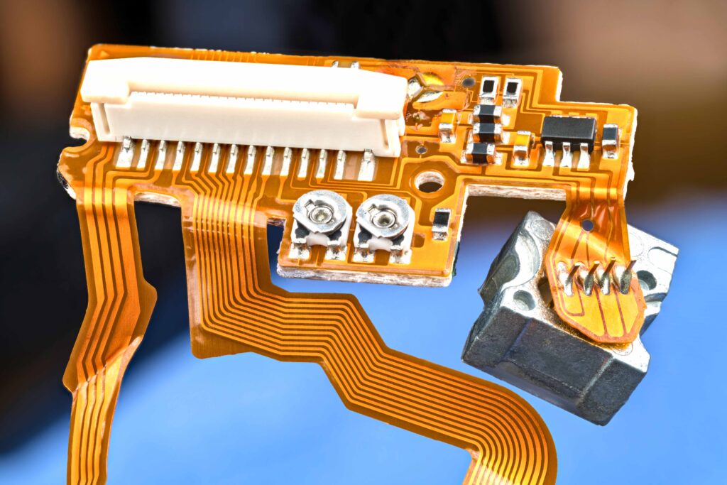
Flexible PCB layout design involves designing PCBs that can bend and flex, making them suitable for applications where traditional rigid PCBs are not practical.
Key Features
– Flexibility: Ability to bend and conform to various shapes.
– Lightweight: Reduced weight compared to rigid PCBs.
– Space Saving: Can fit into compact and irregular spaces.
– Durability: Resistant to vibration and mechanical stress.
Design Considerations
– Bend Radius: Ensuring the PCB can bend without damage.
– Trace Layout: Designing traces to withstand flexing.
– Material Selection: Choosing materials that offer flexibility and durability.
– Thermal Management: Ensuring efficient heat dissipation in flexible designs.
Applications
– Wearable Technology: Smartwatches, fitness trackers, medical devices.
– Consumer Electronics: Foldable smartphones, flexible displays.
– Automotive Electronics: Flexible circuits in dashboards and interior lighting.
– Medical Devices: Compact and flexible circuits in diagnostic equipment.
18. Rigid-Flex PCB Layout
Rigid-flex PCB layout involves designing PCBs that combine both rigid and flexible sections. These designs offer the advantages of both rigid and flexible PCBs, making them suitable for complex applications.
Key Features
– Combination of Rigid and Flexible Sections: Provides structural support and flexibility.
– Space Efficiency: Allows for compact and complex designs.
– Durability: Resistant to vibration and mechanical stress.
– Improved Performance: Reduced number of connectors and interconnections.
Design Considerations
– Transition Areas: Designing smooth transitions between rigid and flexible sections.
– Material Selection: Choosing materials that support both rigidity and flexibility.
– Thermal Management: Ensuring efficient heat dissipation in rigid-flex designs.
– Signal Integrity: Maintaining signal integrity across rigid and flexible sections.
Applications
– Aerospace and Defense: Complex circuits in avionics and military equipment.
– Medical Devices: Compact and flexible circuits in diagnostic and monitoring equipment.
– Consumer Electronics: Foldable smartphones, flexible displays.
– Automotive Electronics: Complex circuits in dashboards and interior lighting.
19. PCB Layout for High Current
PCB layout for high current involves designing PCBs to handle high levels of electrical current without overheating or causing damage to components.
Key Considerations
– Trace Width and Thickness: Ensuring traces can carry high current without excessive heat.
– Thermal Management: Using heat sinks, thermal vias, and copper planes to dissipate heat.
– Component Selection: Choosing components that can handle high current.
– Power Distribution: Designing efficient power distribution to prevent hotspots.
Importance
Designing PCBs for high current is crucial for applications that require robust power delivery. Proper design ensures reliable operation and prevents damage to components.
Applications
– Power Electronics: Power supplies, converters, and inverters.
– Automotive Electronics: High-current circuits in electric vehicles and power management systems.
– Industrial Equipment: High-power machinery and control systems.
– Consumer Electronics: High-current circuits in gaming consoles and high-performance computing.
20. PCB Layout for Low Noise
PCB layout for low noise involves designing PCBs to minimize electrical noise and interference, ensuring clean and reliable signal transmission.
Key Techniques
– Grounding: Providing a stable ground reference to reduce noise.
– Shielding: Using shielding to block external noise sources.
– Filtering: Adding filters to suppress unwanted signals.
– Trace Layout: Designing traces to minimize noise and interference.
Importance
Minimizing noise is essential for the reliable operation of sensitive electronic circuits. Low-noise designs ensure clean signal transmission and prevent data corruption.
Applications
– Medical Devices: Ensuring reliable operation of diagnostic and monitoring equipment.
– Telecommunications: Maintaining signal quality in communication devices.
– Consumer Electronics: Ensuring reliable performance of smartphones, tablets, and laptops.
– Automotive Electronics: Minimizing noise in advanced driver-assistance systems (ADAS).
21. PCB Stack-Up Design
PCB stack-up design involves arranging the layers of a multilayer PCB to optimize performance, signal integrity, and manufacturability.
Key Considerations
– Layer Arrangement: Designing the order and function of each layer.
– Signal Integrity: Ensuring clean signal transmission through controlled impedance.
– Thermal Management: Designing layers for efficient heat dissipation.
– Power and Ground Planes: Providing stable power and ground connections.
Importance
A well-designed stack-up is essential for achieving the best possible performance and reliability. It impacts signal integrity, thermal performance, and the overall manufacturability of the PCB.
Applications
– High-Performance Computing: Optimizing stack-up for data centers and supercomputers.
– Telecommunications: Enhancing performance of communication equipment.
– Consumer Electronics: Improving reliability and performance of smartphones, tablets, and laptops.
– Automotive Electronics: Ensuring optimal performance in vehicle systems.
22. PCB Layout for High Density Interconnect (HDI)
PCB layout for high density interconnect (HDI) involves designing PCBs with a high component density and fine trace widths, allowing for compact and complex designs.
Key Features
– Fine Trace Widths and Spacing: Enabling high component density.
– Microvias: Using small vias for inter-layer connections.
– Blind and Buried Vias: Vias that do not pass through the entire board.
– Multiple Layer Stack-Up: Complex layer arrangements for high-density designs.
Design Considerations
– Signal Integrity: Ensuring clean signal transmission in high-density designs.
– Thermal Management: Efficient heat dissipation in compact designs.
– Manufacturability: Ensuring the design can be reliably manufactured.
– Testing and Inspection: Verifying the integrity of high-density designs.
Applications
– Consumer Electronics: High-density designs in smartphones, tablets, and laptops.
– Medical Devices: Compact and complex circuits in diagnostic equipment.
– Telecommunications: High-density designs in communication equipment.
– Automotive Electronics: Advanced designs in vehicle systems.
23. PCB Layout Testing and Verification
PCB layout testing and verification involves thoroughly testing and validating the PCB design to ensure it meets all requirements and functions correctly.
Key Techniques
– Design Rule Checking (DRC): Ensuring the design meets all manufacturing constraints.
– Electrical Rule Checking (ERC): Verifying the electrical correctness of the design.
– Signal Integrity Analysis: Checking for signal integrity issues.
– Thermal Analysis: Ensuring adequate heat dissipation.
Importance
Thorough testing and verification are essential for identifying and correcting errors before manufacturing. This process reduces the risk of defects, improves yield, and ensures the reliability of the final product.
Applications
– Prototyping: Ensuring prototypes are free from design errors.
– Mass Production: Reducing the risk of defects in large-scale manufacturing.
– Custom Projects: Verifying specialized designs.
– High-Performance Electronics: Ensuring optimal performance and reliability.
24. PCB Layout Documentation
PCB layout documentation involves creating detailed documentation of the PCB design, including schematics, layouts, and assembly instructions. This documentation is essential for manufacturing and assembly.
Key Components
– Schematics: Detailed circuit diagrams of the design.
– Layout Files: Detailed layouts of the PCB design.
– Bill of Materials (BOM): List of all components used in the design.
– Assembly Instructions: Detailed instructions for assembling the PCB.
Importance
Comprehensive documentation is essential for ensuring the design can be accurately manufactured and assembled. It provides all the necessary information for production and helps identify and correct errors.
Applications
– Prototyping: Providing detailed documentation for prototype manufacturing.
– Mass Production: Ensuring accurate and efficient production of large quantities.
– Custom Projects: Documenting specialized designs for unique applications.
– High-Performance Electronics: Providing detailed documentation for complex designs.
25. Automated PCB Layout Design
Automated PCB layout design involves using advanced software tools and algorithms to automate the PCB design process. Automation improves efficiency, reduces errors, and speeds up the design process.
Key Features
– Automated Routing: Automatically routing traces between components.
– Design Rule Checking (DRC): Automatically checking for design rule violations.
– Component Placement: Automated placement of components.
– Simulation and Analysis: Automated signal integrity and thermal analysis.
Importance
Automated PCB layout design improves efficiency and reduces the risk of errors. It speeds up the design process and ensures the design meets all requirements and constraints.
Applications
– Prototyping: Quickly developing and testing new designs.
– Mass Production: Efficiently designing for large-scale manufacturing.
– Custom Projects: Automating specialized designs for unique applications.
– High-Performance Electronics: Automating complex and high-speed designs.
Conclusion
In conclusion, mastering circuit board layout design is crucial for developing efficient and reliable electronic devices. By applying the principles and techniques discussed in this guide, you can enhance the functionality and manufacturability of your PCBs, whether for consumer electronics, automotive systems, or advanced medical devices. Staying updated with the latest trends and tools in PCB design will empower you to tackle complex projects and innovate in your designs. Ultimately, a well-designed PCB serves as the backbone of any successful electronic application, ensuring optimal performance and reliability in a competitive market.