
The Printed Circuit Board (PCB) is an integral component of modern electronics, acting as the foundation upon which nearly every electronic device is built. From its conceptual origins to the advanced technology we see today, PCB and PCB design have undergone significant evolution, transforming from rudimentary designs to complex, miniature, and high-density systems that power everything from mobile phones to wearable devices. This article explores the evolution of PCBs and how their technology has improved over time.
Early Concept and Inception of Printed Circuit Board
The concept of the PCB emerged in the early 20th century when engineers sought a way to organize electrical circuits more efficiently. Prior to PCBs, electrical circuits were constructed using point-to-point wiring, which involved connecting components directly with wires. This approach was labor-intensive, error-prone, and resulted in bulky devices that were difficult to manufacture consistently.
In 1936, Austrian inventor Paul Eisler is credited with creating the first PCB as part of a radio set, marking a pivotal moment in electronics history. His design utilized copper foils etched onto an insulating board to create electrical connections. Initially, the concept faced resistance, but during World War II, PCBs gained attention for their use in military applications, such as in proximity fuses for bombs. This development sparked interest in the broader adoption of the technology.
Post-War Development and Commercialization
After World War II, the commercial potential of PCBs became more apparent. In the 1950s and 1960s, as consumer electronics began to grow, so did the demand for efficient and reliable circuit designs. Transistors replaced bulky vacuum tubes, leading to smaller, more compact devices. PCBs played a key role in this miniaturization, as their layered structure allowed for more efficient use of space.
At this stage, PCBs were primarily single-sided, with all components and connections placed on one side of the board. However, the growing complexity of electronics, especially in industries such as telecommunications and defense, demanded more sophisticated designs.
The Shift to Double-Sided and Multi-Layer PCBs
By the 1960s and 1970s, double-sided PCBs were introduced. These boards had conductive copper tracks on both sides, allowing for more connections and components to be placed on a single board. The introduction of plated-through holes enabled connections between the two sides, further enhancing the board’s complexity and capability.
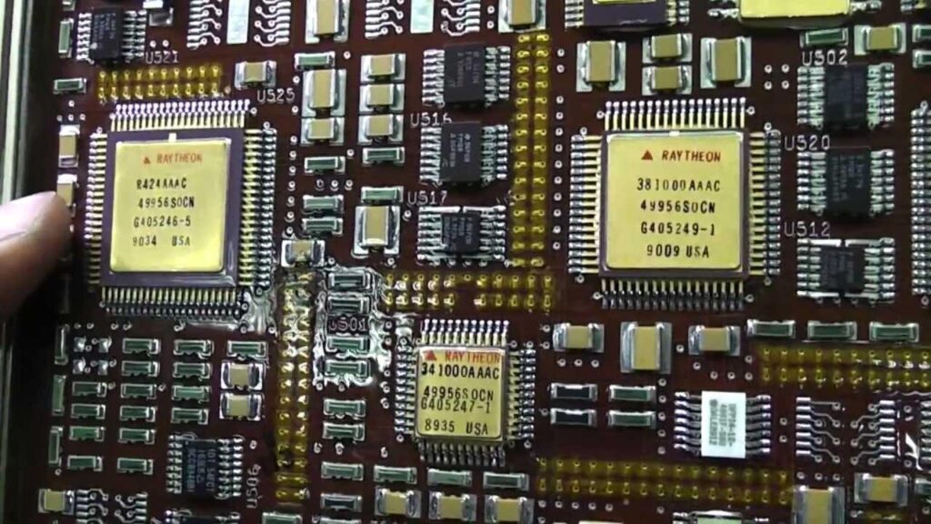
As technology advanced, multi-layer PCBs became the norm. These boards, which consist of multiple layers of conductive material sandwiched between insulating layers, allowed for even greater component density and more intricate circuit designs. The use of multi-layer PCBs was essential in industries like aerospace, telecommunications, and computing, where compactness and performance were critical.
Technological Improvements and Automation
The evolution of PCB technology was closely tied to advances in manufacturing processes. In the 1980s, computer-aided design (CAD) software revolutionized PCB design, allowing engineers to create precise layouts and simulate circuit behavior before manufacturing. This not only improved accuracy but also reduced errors in production.
Automation in PCB manufacturing also made it possible to mass-produce complex designs at lower costs. Techniques like photolithography, where ultraviolet light is used to etch patterns onto the board, became standard practice, further improving the precision and efficiency of PCB production.
Surface-mount technology (SMT), which emerged in the late 1980s and 1990s, was another major breakthrough. Unlike the traditional method of inserting components into holes drilled into the PCB, SMT involves mounting components directly onto the surface of the board. This allowed for even smaller and more densely packed designs, paving the way for the miniaturization of consumer electronics.
The Rise of Miniaturization and High-Density Interconnects
The late 20th century saw an explosion in consumer electronics, with devices like mobile phones, personal computers, and gaming consoles becoming ubiquitous. This trend placed increased demands on PCB technology, particularly in terms of size, power efficiency, and component density.
High-Density Interconnect (HDI) PCBs emerged as a solution to these challenges. HDI technology allows for more connections and smaller components by utilizing finer traces, microvias, and multiple layers of interconnects. This technology made it possible to design and manufacture compact devices with greater functionality.
The trend toward miniaturization has continued into the 21st century, with wearable technology, such as smartwatches and fitness trackers, becoming mainstream. These devices rely on tiny, highly efficient PCBs that can fit into small enclosures while delivering significant processing power and battery life.
Flex and Rigid-Flex PCBs
Another significant advancement in PCB technology is the development of flexible and rigid-flex PCBs. Traditional rigid PCBs are made from solid materials, limiting their use in applications where flexibility is required. Flexible PCBs, on the other hand, are made from flexible materials like polyimide, allowing them to bend and fold to fit into compact and irregular spaces.
Rigid-flex PCBs combine the best of both worlds by incorporating both rigid and flexible sections in a single board. This technology is particularly useful in applications like wearable devices, where flexibility is needed for comfort, but rigidity is required for mounting components.
PCBs in Modern Electronics: Wearables, Mobile Devices, and IoT
The evolution of PCBs has been instrumental in the development of modern electronics. Today, PCBs are at the heart of everything from smartphones and laptops to wearable devices and Internet of Things (IoT) sensors.
Wearable devices, such as smartwatches and fitness trackers, are prime examples of how PCBs have enabled miniaturization. These devices contain tiny PCBs with multiple layers and dense component layouts, all housed in a small, lightweight form factor. Flexible PCBs are often used in wearables to ensure the device can move with the user’s body while maintaining performance and durability.
In mobile phones, PCBs have become increasingly complex and compact, allowing manufacturers to pack more functionality into thinner and lighter devices. High-density interconnects, multi-layer designs, and surface-mount components are essential for the modern smartphone’s small size and advanced features.
High-Density and Future Trends
As technology continues to evolve, so too will PCBs. High-density interconnects will become even more critical as electronics demand faster speeds, higher power efficiency, and more compact designs. Technologies like 5G, artificial intelligence (AI), and autonomous vehicles will push PCB designs to their limits, requiring even greater precision, efficiency, and reliability.
One of the most exciting developments on the horizon is the integration of PCBs with flexible, stretchable, and biocompatible materials. These innovations will drive the next generation of wearable technology, medical implants, and even bioelectronics, where PCBs can be integrated into the human body.
Conclusion
The evolution of the printed circuit board from its early conceptual stages to today’s high-density, miniaturized technology has been remarkable. Over the past century, PCBs have transformed from simple designs used in basic electronics to complex, multi-layered, and flexible systems that power the devices we use daily. As technology continues to advance, PCBs will undoubtedly play a crucial role in shaping the future of electronics, enabling everything from more compact smartphones to the next generation of wearable and IoT devices. We at Arshon Technology will be happy to help with your PCB Design needs.