
In the ever-evolving world of electronics, two essential domains—pcb design and VLSI—often intersect yet serve fundamentally different purposes. While PCB design refers to the physical layout and interconnection of components on a printed circuit board, VLSI (Very Large Scale Integration) refers to the process of embedding thousands to billions of transistors on a single semiconductor chip. These technologies form the backbone of modern electronics, from consumer gadgets to industrial machinery, but each follows its unique design flow, implementation strategy, and field of application. Understanding the distinction between PCB design vs VLSI is crucial for engineers, tech investors, and product developers seeking to optimize electronic systems for performance, cost, or scale.
What is PCB Design?
PCB (Printed Circuit Board) design is the process of creating a layout that electrically connects electronic components using conductive tracks, pads, and other features on a non-conductive substrate. PCBs provide mechanical support and facilitate signal transmission and power delivery across the system. A typical PCB design involves schematic capture, component placement, routing, and design rule checking.
PCBs can range from single-layer to complex multilayer designs with embedded vias and controlled impedance traces, especially in high-speed applications like data centers or automotive systems. PCB designers often work with design software like Altium Designer, Eagle, KiCAD, or OrCAD.
What is VLSI?
VLSI (Very Large Scale Integration) is a subset of microelectronics engineering focused on integrating millions or billions of transistors into a single chip. The primary application of VLSI is the creation of integrated circuits (ICs), such as microprocessors, memory chips, and application-specific integrated circuits (ASICs). VLSI involves digital logic design, synthesis, verification, layout design, and fabrication.
The VLSI design process requires highly specialized tools such as Synopsys, Cadence, or Mentor Graphics and includes multiple stages such as RTL coding (usually in Verilog or VHDL), simulation, place and route, power analysis, and timing closure. VLSI is the heart of chip design, forming the logic core that PCB systems eventually integrate.
PCB Design vs VLSI: Core Differences
| Feature | PCB Design | VLSI |
|---|---|---|
| Level of Integration | Interconnects discrete components | Integrates millions/billions of transistors |
| Design Scale | Board level | Chip level |
| Tools Used | Altium, Eagle, KiCAD | Synopsys, Cadence, Mentor |
| Output | Physical circuit board | Fabricated silicon chip |
| Materials | FR4, Rogers, etc. | Silicon wafers |
| Application Focus | Power distribution, connectivity | Data processing, memory, logic |
| Design Complexity | Medium to high (depends on layers) | Extremely high, nanoscale precision |
| Time to Market | Typically shorter | Longer due to fab processes |
| Cost of Prototyping | Relatively low | Extremely high due to mask and fab |
| Manufacturing Dependency | PCB fabrication house | Semiconductor foundries (TSMC, Intel, etc.) |
Design Flow Comparison
PCB Design Flow:
- Requirement gathering
- Schematic capture
- Footprint assignment
- Component placement
- Routing (manual or auto)
- DRC/ERC checks
- Gerber file generation
- Fabrication and assembly
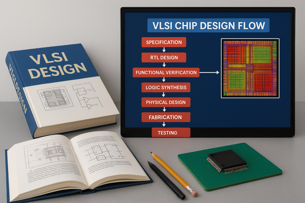
VLSI Design Flow:
- Design specification
- RTL coding
- Functional simulation
- Synthesis
- Floor planning
- Placement and routing
- Static timing analysis
- DRC/LVS checks
- Tape-out and fabrication
PCB design focuses on how signals travel across components already manufactured. In contrast, VLSI design is about creating the internal logic of those components from scratch.
Industry Applications
PCB Design Applications:
- Consumer electronics (phones, TVs)
- Industrial automation
- Automotive ECUs
- Medical devices
- IoT devices
VLSI Applications:
- Microprocessors and GPUs
- FPGAs and SoCs
- AI accelerators
- Memory chips
- Wireless communication chips
In essence, VLSI is about creating the “brains” of an electronic system, while PCB design is about connecting those brains with other components like sensors, power modules, and interfaces.
Skills and Career Paths
PCB Design Engineer:
- Requires knowledge of electronics, signal integrity, EMC/EMI
- Expertise in CAD tools
- Understanding of manufacturing constraints
- Entry to mid-level barrier to entry
VLSI Design Engineer:
- Requires strong digital logic and circuit theory foundation
- Advanced understanding of HDL (VHDL/Verilog)
- Familiarity with EDA tools and semiconductor physics
- High barrier to entry, often requires M.S. or Ph.D.
The choice between these two depends on whether one is more inclined toward hardware systems integration or chip-level innovation.
Cost and Time Considerations
When developing an electronic product, understanding cost and time differences in pcb design vs vlsi can guide project planning.
- PCB Prototyping is faster and cheaper. A 4-layer PCB might take 2–3 days and cost $50–$200 depending on size and quantity.
- VLSI Prototyping is expensive and time-consuming. A single ASIC mask set can cost upwards of $100,000–$1 million and take months to fabricate.
Thus, for startups or quick proof-of-concepts, PCB design is typically the go-to. VLSI is pursued for high-volume products that justify upfront investment.
Co-Design and Collaboration
In many modern products, co-design of PCBs and VLSI chips is essential. For example, in a smartphone:
- The VLSI design team develops the SoC.
- The PCB team integrates the SoC with antennas, power regulators, memory, and I/O.
Such collaborative design requires tight coordination, interface standardization (e.g., SPI, I2C, PCIe), and thermal/power budget management.
Future Trends
PCB Design Trends:
- HDI (High Density Interconnect)
- Flexible PCBs
- Embedded components
- Better thermal management for power electronics
VLSI Trends:
- 3nm and 2nm process nodes
- Chiplet architecture (e.g., AMD’s Ryzen)
- Neuromorphic and quantum computing chips
- Advanced packaging (e.g., 2.5D/3D ICs)
As we move into AI-driven edge computing, both domains are growing together. More powerful chips (VLSI) need better integration and thermal solutions (PCB design).
Which One to Choose?
If you’re developing:
- A wearable health tracker → Start with PCB design, and use existing ICs.
- A new AI accelerator chip → Begin with VLSI and then design a board to host it.
- A startup MVP or industrial controller → PCB design is cheaper, faster, and easier to iterate.
For most electronics, the path is sequential:
- VLSI team creates the chip (logic engine)
- PCB team builds the system around it
They are complementary, not mutually exclusive.
Conclusion
Understanding the pcb design vs vlsi landscape is critical in today’s electronics-driven economy. PCB design provides the infrastructure and interconnection backbone for components, while VLSI design creates the core computational elements. Each field has unique tools, methodologies, and applications, and mastering either (or both) opens up vast opportunities in the electronics industry. Whether you’re a budding engineer, tech entrepreneur, or decision-maker in product development, recognizing the strengths and use cases of each will ensure better technical and business outcomes.