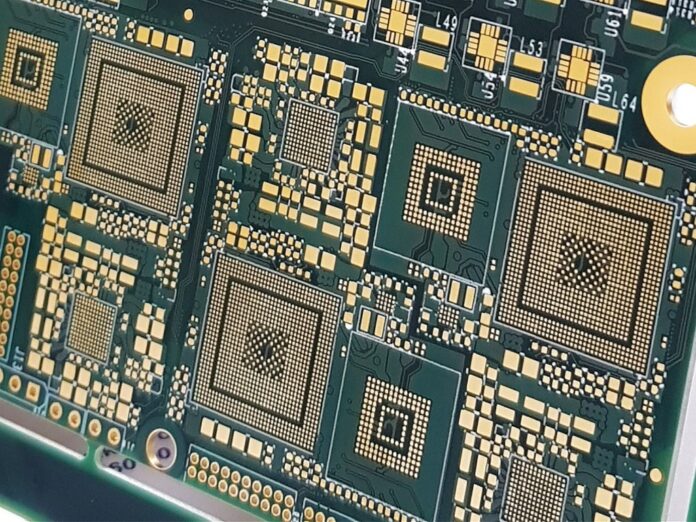
In the world of electronics, the printed circuit board (PCB) serves as the backbone that connects and controls various electronic components. PCBs are essential for virtually all electronic devices, from simple gadgets to complex systems found in smartphones, computers, and industrial machinery. When designing a PCB, engineers often face a critical decision: should they opt for a single-layer or a multi-layer PCB?
This article will delve into the fundamental differences between single-layer and multi-layer PCBs, their respective advantages and disadvantages, and the considerations that influence the choice between the two.
What are PCBs?
Before diving into the specifics of single-layer and multi-layer PCBs, it’s essential to understand what a PCB is and its purpose. A printed circuit board is a flat board made of insulating material (usually fiberglass or epoxy resin) with conductive pathways etched onto its surface. These pathways serve as electrical connections between the various components, allowing them to communicate and function as intended. PCBs can vary in complexity and layout, often consisting of various layers, including traces, pads, and vias.
Single-Layer PCBs
Single-layer PCBs, also known as single-sided PCBs, are the simplest type of PCBs. They consist of one conductive layer, usually made of copper, that is applied to one side of the board. The components are mounted on the top side, while the opposite side remains free of any traces or pads.
Advantages of Single-Layer PCBs
Simplicity
The design of single-layer PCBs is straightforward. Because there is only one layer of traces, the layout process is more intuitive, making it easier to design and fabricate.
Cost-Effectiveness
Single-layer PCBs generally cost less to manufacture than their multi-layer counterparts. This is due to the simpler fabrication process and fewer materials required.
Ease of Production
With a single layer, the PCB can be produced quickly, allowing for shorter lead times in manufacturing.
Easy Debugging and Repair
Troubleshooting issues on single-layer PCBs is typically easier, as components and traces are more accessible. If a fault occurs, it is often easy to identify and rectify.
Disadvantages of Single-Layer PCBs
Limited Space
A significant drawback of single-layer PCBs is their limited space for traces and components. The single layer may become overcrowded with traces, making it challenging to fit a large number of components.
Higher Electromagnetic Interference (EMI)
The simplicity of single-layer designs can lead to increased electromagnetic interference compared to multi-layer designs. This can impact performance in sensitive electronic applications.
Routing Limitations
With only one layer for routing, engineers must be more creative in their designs, which can sometimes lead to suboptimal layouts.
Multi-Layer PCBs
Multi-layer PCBs, as the name implies, consist of multiple layers of conductive material that are stacked and bonded together. These layers can be designed to improve connections and signal integrity, making them a popular choice for complex electronic applications.
Advantages of Multi-layer PCBs
Increased Component Density
Multi-layer PCBs allow for a much higher density of components due to the availability of multiple layers for routing. This is particularly beneficial for devices with complex circuitry, such as smartphones and computers.
Improved Signal Integrity
By using multiple layers, designers can implement better signal routing techniques, minimizing the risk of crosstalk and electromagnetic interference. This leads to enhanced overall performance.
More Design Flexibility
Multi-layer PCBs offer more flexibility in terms of layout and design. Engineers can allocate different layers for power, ground, and signal paths, allowing for optimized performance.
Compact Design
With the ability to fit more components into a smaller space, multi-layer PCBs are ideal for compact devices where space is at a premium.
Disadvantages of Multi-layer PCBs
Higher Cost
One of the primary disadvantages of multi-layer PCBs is their increased manufacturing cost. The complexity of design and production leads to higher expenses.
Manufacturing Complexity
Multi-layer PCBs require more intricate production processes, which can lead to longer lead times and potential manufacturing defects.
Difficulties in Repair
Debugging and repairing multi-layer PCBs can be challenging due to their complex design. It may be difficult to access specific layers, making it hard to diagnose issues.
Longer Design Time
Designing a multi-layer PCB often takes longer than a single-layer design due to the added complexity and considerations involved in layer stacking and routing.
Key Factors in Choosing Between Single-Layer and Multi-Layer PCBs
When choosing between single-layer and multi-layer PCBs, several factors come into play. Understanding these factors can help engineers and designers make informed decisions based on the specific needs of their projects.
Complexity of the Circuit
The complexity of the circuit is one of the most significant considerations. Simple circuits with fewer components may be best suited for single-layer PCBs. In contrast, complex circuits with numerous components and connections may necessitate a multi-layer approach.
Available Space
Available space is another critical factor. For compact devices, multi-layer PCBs can accommodate more components within a smaller footprint. However, if space allows, and the circuit is simple, a single-layer PCB might suffice.
Performance Requirements
Performance is often a key consideration. High-frequency applications or those sensitive to interference benefit from the enhanced signal integrity provided by multi-layer PCBs. For less demanding applications, a single-layer PCB may perform adequately.
Constraints
Companies must consider their budget when choosing a PCB type. Single-layer PCBs are more cost-effective, which may be vital for projects with tight budgets. However, investing in a multi-layer PCB could ensure better performance and reliability for critical applications.
Production Volume
The expected production volume can also influence the choice between single-layer and multi-layer PCBs. High-volume production of simpler devices may benefit from single-layer designs, while low-volume production of complex devices may justify the higher costs associated with multi-layer PCBs.
Repairability
If the product is designed to be repaired easily, single-layer PCBs are usually the most accessible option. On the other hand, multi-layer PCBs might complicate repairs due to the intricacies of multiple layers.
Conclusion: Choosing the Right PCB Solution

In conclusion, the choice between single-layer and multi-layer PCBs is influenced by a variety of factors, including circuit complexity, available space, performance needs, budget constraints, production volume, and repairability. Single-layer PCBs are ideal for straightforward, cost-effective applications where production and repair ease are priorities. Conversely, multi-layer PCBs excel in high-density, complex applications that require enhanced signal integrity and design flexibility, despite their higher cost and manufacturing intricacies.As a leader in PCB design and manufacturing, Arshon Technology is committed to delivering high-quality solutions tailored to meet the unique demands of each project. By meticulously evaluating the specific requirements of a project, engineers and designers can make informed decisions that enhance the reliability and functionality of their electronic products. Understanding the distinct characteristics of both single-layer and multi-layer PCBs is essential for navigating the evolving landscape of electronics and achieving excellence in performance and innovation.
