
Introduction
When it comes to electronic design, the demand for more complex functionality, higher speed, and compact packaging has paved the way for multi-layer printed circuit boards (PCBs). While 2-layer and 4-layer boards remain common in simpler applications, the trend toward more intricate designs with greater signal integrity requirements has made 8 layer PCBs increasingly popular. An 8 layer PCB offers a robust platform for routing complex signals, managing ground and power layers effectively, and providing improved electromagnetic interference (EMI) performance.
This article delves into all aspects of an 8 layer PCB—from 8 layer pcb stackup considerations and 8 layer pcb thickness to layout examples and PCB board material choices. Whether you are a seasoned engineer or new to PCB design, understanding the complexities of an 8 layer PCB can be instrumental for modern electronic design.
1. 8 Layer PCB Stackup
Why Stackup Matters
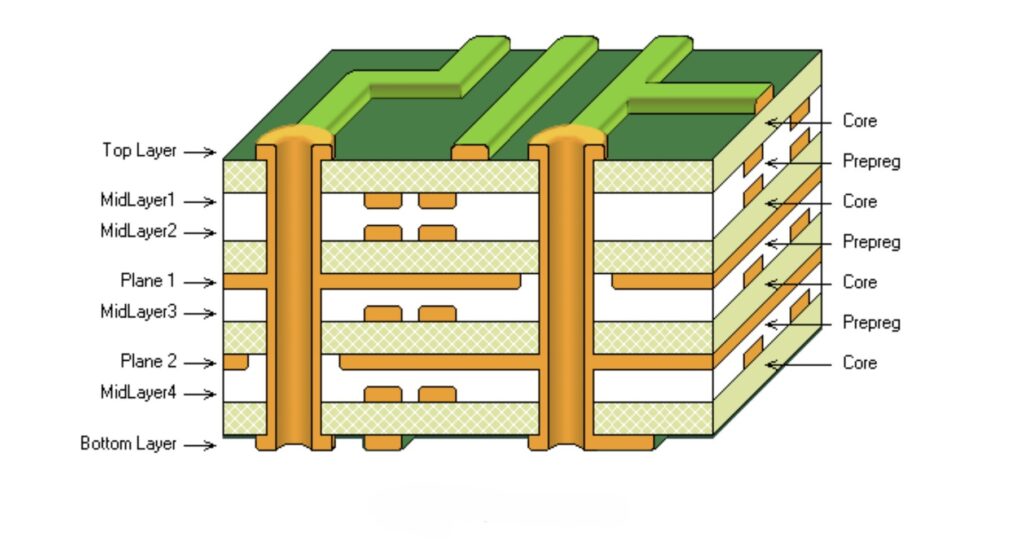
The term “stackup” refers to the arrangement and sequence of conductive (copper) and non-conductive (dielectric) layers within a multi-layer PCB. A well-conceived 8 layer pcb stackup serves several key objectives:
- Signal Integrity: Placing high-speed signal layers adjacent to continuous reference planes (ground or power planes) minimizes noise and crosstalk.
- EMI/RFI Control: Proper stacking can trap or redirect unwanted electromagnetic emissions, improving regulatory compliance and reducing interference within the board.
- Thermal Management: Distributing copper planes and choosing the right PCB board material help dissipate heat more effectively.
- Reliability: A balanced stackup with symmetrical layers reduces warping during manufacturing and in operation, boosting the board’s mechanical stability.
Typical 8 Layer PCB Stackup Configuration
While each electronic design may need a customized arrangement, a common 8 layer pcb stackup might look like this:
- Top Layer (Signal)
- Ground Plane (GND)
- Internal Layer 1 (Signal or Power)
- Internal Layer 2 (Signal or Power)
- Internal Layer 3 (Power Plane)
- Ground Plane (GND)
- Internal Layer 4 (Signal)
- Bottom Layer (Signal)
In many designs, the power plane (or multiple power planes) is placed near the center to provide a solid reference and minimize noise. Ground planes are often placed directly adjacent to high-speed or sensitive signal layers, ensuring that any return currents have a low-impedance path.
Considerations for Layer Assignments
- High-Speed Signals: Place them close to ground planes for better noise suppression.
- Power Distribution: Use one or more dedicated planes to distribute different voltages. This approach reduces noise, improves current capacity, and simplifies decoupling strategies.
- Sensitive Analog Regions: If your design includes analog circuitry, keep analog signals separate from noisy digital signals.
- Electromagnetic Compatibility (EMC): EMI performance is strongly tied to having continuous, uninterrupted reference planes beneath critical signals.
A well-structured 8 layer pcb stackup balances these factors, ensuring that your design remains stable, reliable, and capable of meeting performance targets.
2. 8 Layer PCB Example
Practical Usage in Modern Electronics
An 8 layer pcb offers substantial routing space and dedicated planes, making it an excellent choice in the following scenarios:
- Motherboards and PC Components: Where numerous high-speed buses (PCIe, USB 3.x, SATA) need careful routing and controlled impedance.
- Telecommunications Equipment: Routers, switches, and base stations often employ multiple power rails and high-speed network interfaces.
- FPGA and SoC Boards: With extensive I/O pin counts, large data buses, and specialized power planes for different internal modules.
- Advanced Embedded Systems: Single-board computers and industrial control units that integrate CPU modules, graphics, and networking on one board.
Example Layout: A Hypothetical Application
Suppose you’re designing a high-end embedded system board with the following requirements:
- A powerful System-on-Chip (SoC) running at 1–2 GHz
- Multiple memory interfaces (DDR4 or LPDDR4) requiring matched trace lengths
- PCI Express lanes and other high-speed serial interfaces
- Separate power rails for core logic, I/O, and analog subsystems
In an 8 layer pcb:
- Top Layer (L1) might host critical high-speed signals for the SoC and memory lines.
- Layer 2 (L2) could be a ground plane adjacent to the top layer to maintain tight coupling and reduce crosstalk.
- Layer 3 (L3) and Layer 4 (L4) might carry power distribution and moderate-speed signals.
- Layer 5 (L5) might be another dedicated ground plane or an additional power plane.
- Layer 6 (L6) could be used for routing differential pairs for PCIe or other data lines.
- Layer 7 (L7) again might be a ground or specialized plane (e.g., analog ground) if needed.
- Bottom Layer (L8) is another signal layer for completing routing, breakout lines, or lower-speed connections.
With this example, you achieve robust EMI performance, minimized crosstalk, and a clean power distribution network, all while accommodating a large number of signals.
3. 8 Layer PCB Thickness
Factors Influencing PCB Thickness
The total thickness of an 8 layer pcb depends on multiple factors, including:
- Core and Prepreg Materials: The thickness of the dielectric layers (prepregs) between copper layers significantly influences the final thickness.
- Copper Weight: Common copper thickness options range from 0.5 oz to 2 oz. Heavier copper adds to the overall thickness.
- Finished Layer Count: Having 8 conductive layers plus the outer solder mask and surface plating all contribute to the final board thickness.
- Manufacturer Capabilities: Some PCB manufacturers may offer micro-thin cores or specialized prepregs, reducing thickness. Others might have standard thickness ranges.
Standard Thickness Ranges
For an 8-layer stackup, typical thicknesses might lie between 1.57 mm (0.062 in.) and 2.36 mm (0.093 in.). Some high-density interconnect (HDI) boards or advanced PCB design can push final thicknesses below 1 mm for extremely compact applications, but this usually involves specialized processes and higher costs.
Why Thickness Matters
- Impedance Control: The spacing between signal layers and their reference planes directly affects characteristic impedance. Thinner dielectrics can make controlling impedance simpler but may also raise concerns about manufacturing yields.
- Mechanical Strength: A thicker board is more rigid, providing better durability in harsh environments or mechanically stressful applications.
- Connectors and Mounting: Some connectors and mechanical fixtures are designed around a particular board thickness. Incompatible thickness can cause assembly or reliability issues.
Striking the right balance in 8 layer pcb thickness is a key part of PCB design. It ensures you achieve the necessary mechanical rigidity, impedance requirements, and manufacturing feasibility.
4. 8 Layer PCB Dimensions
How to Determine Board Dimensions
Board dimensions refer to the overall length and width of the PCB, typically measured in millimeters (mm) or inches. Determining the size of an 8 layer pcb involves:
- Component Placement: Large connectors, modular headers, or heat sinks may define the board’s minimum length or width.
- Enclosure Constraints: For products enclosed in a specific casing, the PCB must fit within predetermined boundaries.
- Panelization Requirements: Manufacturers often produce multiple boards in a single panel. Efficient panel utilization can reduce costs.
- Routing Density: If the design calls for tight pitch components (e.g., BGAs), you may require more board space to accommodate breakout areas without excessive complexity.
Balancing Compactness with Manufacturability
Engineers often want to minimize board size to reduce cost and keep the product footprint small. However, shrinking dimensions can complicate routing, particularly in a design with 8 layers. You must ensure that each layer’s constraints—like via-in-pad technology or track width—are feasible given your chosen PCB board material and manufacturing partner’s capabilities.
Typical Dimensions in Practice
- Standard Motherboard Form Factors: For instance, an ATX motherboard might measure 305 x 244 mm. Mini-ITX boards are around 170 x 170 mm. These are more relevant for an 8 layer PCB motherboard scenario.
- Embedded Systems or Development Boards: Boards can vary from as small as 100 x 100 mm to 200 x 150 mm, depending on the complexity.
- Custom Industrial Designs: Dimensions may be driven entirely by the mechanical enclosure or the layout of the end-product.
Ultimately, 8 layer pcb dimensions must strike a balance between your layout needs, cost targets, and mechanical constraints.
5. 8 Layer PCB Stackup Altium
Using Altium Designer for an 8 Layer PCB Stackup
Altium Designer is a leading electronic design software platform well-suited for complex, multi-layer PCB projects. Setting up an 8 layer pcb stackup in Altium involves:
- Layer Stack Manager: This feature allows you to define the number of signal layers, copper thickness, dielectric materials, and even advanced structures like rigid-flex segments if needed.
- Dielectric Definitions: Altium lets you specify the exact thickness and dielectric constant (Dk) of each layer of prepreg or core. This is crucial for controlled impedance design.
- Impedance Profiles: You can create impedance profiles for single-ended and differential pairs. Altium automatically calculates the required trace width and spacing based on the chosen materials and layer stack.
- Layer Pairing: Typically, symmetrical stackups are beneficial. Altium can help you manage symmetrical layering to minimize mechanical stresses.
Tips for Effective Design in Altium
- Keep Layers Organized: Name each layer clearly (e.g., “Top Signal,” “GND Plane,” “Internal Power”).
- Use Design Rules: Implement Altium’s rules for track widths, clearances, via sizes, and plane connections.
- Conduct Stackup Validation: Altium can alert you to potential issues with impedance or missing reference planes.
- Utilize 3D Visualization: Altium’s 3D mode helps confirm that your 8-layer design will fit enclosures and connectors correctly.
Choosing the right PCB board material in Altium’s Layer Stack Manager also ensures that your final physical board aligns with the software’s electrical simulations and mechanical representations.
6. 8 Layer PCB Motherboard
Why Motherboards Often Use 8 Layers (or More)
A motherboard is the central hub in a computer or a comparable modular system, hosting critical components like the CPU, memory, expansion slots, and power regulators. Given the high complexity and myriad signals involved:
- Multiple Voltage Rails: Separate layers for various power domains help isolate noise-sensitive sections (e.g., CPU power vs. peripheral power).
- High-Speed Interfaces: PCIe, USB, SATA, and other buses demand carefully controlled impedance and tight coupling to ground planes to minimize data errors.
- Thermal Management: Copper planes can be utilized to spread heat more evenly, critical in high-power components.
- Densely Packed Components: An 8 layer pcb provides the real estate for breakout and routing even when the motherboard is physically large.
Typical Stackup for a Motherboard
A typical 8 layer pcb motherboard stack might look like:
- Layer 1: Top Signal (High-speed CPU or memory signals)
- Layer 2: Ground Plane
- Layer 3: Internal Signals (Peripheral or slower signals)
- Layer 4: Power Plane
- Layer 5: Power Plane or another Ground Plane
- Layer 6: Internal Signals (Expansion slots, chipset connections)
- Layer 7: Ground Plane
- Layer 8: Bottom Signal (I/O connectors, interface lines)
Some motherboards use 6 layers, while high-end models could go to 10 or even more layers, depending on advanced CPU sockets and chipset requirements.
PCB Board Material Considerations for Motherboards
Choosing the right PCB board material is essential in a motherboard:
- Thermal Performance: High-Tg FR-4 or specialized laminates may be required to handle heavy CPU power and repeated thermal cycles.
- Signal Integrity: Low-loss materials (e.g., improved FR-4 or high-speed laminates like Megtron or Rogers) might be used for premium motherboards running at higher data rates.
- Cost vs. Performance: Consumer motherboards often balance cost with performance by using standard FR-4, while gaming or server-grade motherboards might use more advanced laminates.
Additional Considerations for an 8 Layer PCB
Material Selection
- FR-4: A common, cost-effective PCB board material used across multiple industries. For high-speed or high-temperature designs, a high-Tg variant is recommended.
- Rogers or Advanced Laminates: Often chosen for ultra-high-speed RF or network applications where low dielectric loss is paramount.
- Polyimide: Used for flexible circuits or in rigid-flex solutions, if certain layers in the stack require flex.
Via Technologies
Multi-layer boards rely heavily on vias to connect signals and planes across layers:
- Through-Hole Vias: Drilled through all eight layers; simplest but can consume significant routing space.
- Blind/Buried Vias: Connect only specific layers, enabling more efficient routing in high-density designs.
- Via-in-Pad: Sometimes used for BGAs with fine pitches, placing vias directly in the component pads and capping them for smooth soldering surfaces.
Thermal Management
Effective thermal management is critical in multi-layer boards:
- Copper Planes: Inner layers used as ground or power planes also function as heat spreaders.
- Thermal Vias: Arrays of vias near heat-generating components (e.g., voltage regulators) help conduct heat to inner layers or a heatsink.
- Heat Dissipation Layers: Some advanced designs incorporate metal cores or thicker copper for better thermal transfer.
Manufacturing and Assembly Costs
With each additional layer, complexity in PCB manufacturing and assembly rises. Factors influencing cost include:
- Number of Drill Hits: More vias and specialized via processes (like blind and buried) drive up costs.
- Inspection and Testing: Additional layers complicate automated optical inspection (AOI) and X-ray testing.
- Yield Rates: Tight tolerances can reduce yields, especially in designs pushing the envelope for trace width/spacing or via dimensions.
Conclusion
The transition to an 8 layer pcb can offer a host of advantages—improved signal integrity, enhanced EMI performance, and a more organized approach to distributing power and grounding. However, these boards require careful planning in terms of stackup, thickness, and overall PCB design. Whether it’s a motherboard packed with high-speed interfaces, a data-intensive embedded system, or a telecommunications device needing multiple power rails, an 8 layer pcb can address complex electronic design challenges that simpler boards simply cannot manage effectively.
In addition, understanding how to select the correct PCB board material and how to optimize layer stackups—especially using tools like Altium—will help ensure robust performance and efficient manufacturability. While they demand a higher budget and advanced manufacturing considerations, 8-layer boards can be the difference between a high-performance, stable product and one that struggles with electromagnetic interference or signal integrity issues.
Ultimately, the decision to move to an 8 layer pcb is a strategic one: balancing cost, complexity, and the stringent demands of modern electronic design. With proper planning, well-chosen materials, and rigorous design rules, you can unlock the full potential of an 8-layer stackup, thereby creating cutting-edge products that excel in reliability, speed, and overall performance.