
Printed Circuit Boards (PCBs) are the backbone of modern electronics, connecting and supporting components in a vast array of devices. One of the critical elements in PCB design that enable this connectivity between components is the via. PCB Vias are used to connect the various layers of a multi-layer PCB, ensuring that signals, power, and ground connections flow seamlessly across the board. Without vias, it would be nearly impossible to design and manufacture the complex electronic systems we rely on today.
In this article, we’ll explore what PCB vias are, the different types of vias, and their significance in the design and functionality of modern PCBs.
What Are PCB Vias?
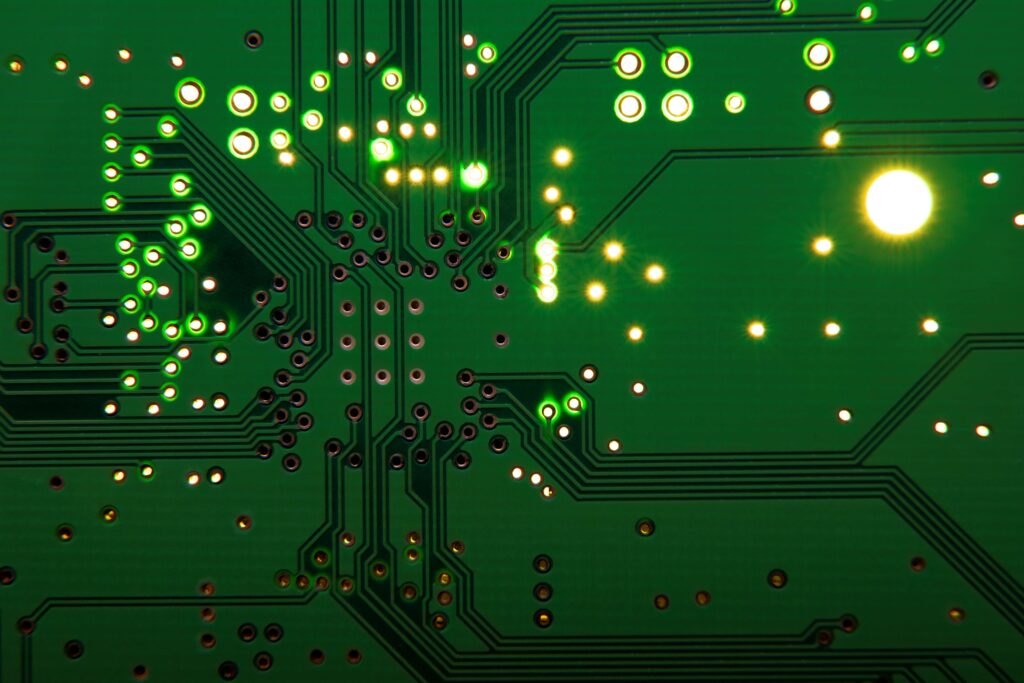
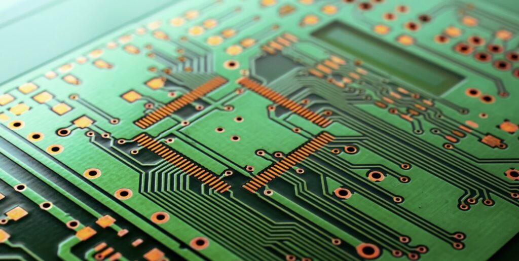
A via is a small hole or passage through a PCB that allows electrical signals to travel from one layer to another. PCBs can have multiple layers, with each layer serving a specific function (such as power distribution, ground planes, or signal routing). Vias create vertical interconnections between these layers, enabling complex, multi-layer designs.
PCB Vias are crucial because they help maintain the integrity of the circuit design while minimizing the space required for connections. Without vias, the circuit layout would be significantly more challenging, and more space would be needed for connections between components. As PCBs continue to evolve, especially with the increasing demand for compactness and complexity in consumer electronics, vias play a more essential role in efficient design and manufacturing.
How Do Vias Work?
In a PCB, layers are typically separated by insulating material, and vias are used to create conductive pathways between them. A via is made by drilling a hole through the PCB layers, and then a thin layer of copper is plated on the walls of the hole. The copper plating makes the via electrically conductive, allowing signals or power to flow between the layers.
When a PCB is manufactured, the via is typically filled with a conducting material (often copper) that connects the layers, allowing electrical signals to pass through. This makes vias an essential component for creating the connectivity between different layers of the board.
Vias also play a role in the signal integrity and performance of the PCB. The size, type, and placement of vias impact the electrical properties of the board, such as resistance, inductance, and capacitance. In high-speed or high-frequency circuits, vias are carefully designed to minimize signal loss and ensure high performance.
Types of PCB Vias
There are several types of vias, each with its own applications and benefits. The primary types of vias include:
Through-hole Vias
Through-hole vias are the most common type of vias used in PCB design. They pass through the entire thickness of the PCB, connecting the top and bottom layers of the board. Through-hole vias are used in designs where a simple connection between layers is required.
Through-hole vias are typically larger than other types of vias, which makes them easier to manufacture. They also allow for the placement of components with leaded connections on both sides of the PCB, which is particularly useful in through-hole mounting technology. However, they can take up more space on the PCB compared to other types of vias.
Blind Vias
Blind vias are used to connect the outer layers of a PCB to one or more inner layers, but they do not pass all the way through the board. These vias only extend from the surface to one or more internal layers and are “blind” to the opposite side of the board.
Blind vias are often used in multi-layer PCBs to reduce the number of layers needed, allowing the PCB to remain compact while still providing the necessary connectivity between layers. They are often smaller and more precise than through-hole vias, which can help save space on the PCB.
Buried Vias
Buried vias are similar to blind vias in that they are used to connect inner layers without passing through the outer layers. However, buried vias are unique because they only appear in the internal layers of the PCB and are not visible from the surface. They are used when connecting two or more inner layers without creating any unnecessary external vias.
Buried vias are more complex to manufacture than blind vias because they are typically created through a series of additional drilling and plating processes. However, they are highly beneficial for dense, high-layer-count PCBs, as they can reduce the overall size of the board and increase the available real estate for components.
Micro Vias
Micro vias are extremely small vias typically used in high-density interconnect (HDI) PCBs, which are used in devices like smartphones and tablets. Micro vias are typically created using laser drilling and are often used in multi-layer boards where space is at a premium.
The primary advantage of micro vias is their ability to reduce the size of the PCB while still maintaining the necessary electrical connections between layers. This is particularly important for modern electronics, where miniaturization and high-speed performance are critical.
Via-in-Pad
Via-in-pad refers to a design where a via is placed directly under a component pad, which is the area on the PCB where a component is mounted. This is usually done in advanced PCB designs to save space or improve performance.
Via-in-pad technology is commonly used in high-frequency, high-performance applications, such as radio frequency (RF) or high-speed digital circuits. However, this design can create challenges in the manufacturing process, as the via must be carefully managed to avoid issues with soldering or the structural integrity of the component.
The Role of Vias in PCB Design
Vias are not just used for connecting layers; they also play a role in enhancing the overall design of a PCB. Some of the key roles of vias in PCB design include:
Reducing Board Size
Vias allow designers to connect different layers of the board without needing to place traces on the outer layers. By connecting multiple layers of the PCB, vias help reduce the size of the board, allowing for a more compact design. This is particularly useful in consumer electronics, where space is limited.
Improving Electrical Performance
Vias can be strategically placed to improve the performance of a PCB. For example, vias are often used to connect ground planes and power distribution layers, which helps reduce noise and ensures the stability of the signals. This is critical in high-speed or high-frequency circuits where signal integrity is paramount.
Heat Dissipation
Vias can also serve as heat sinks by connecting heat-sensitive areas of the PCB to heat-dissipating layers, such as copper planes. This helps to spread the heat generated by components, preventing overheating and ensuring that the PCB functions efficiently.
Signal Routing and Space Saving
Vias are often used to route signals across multiple layers, enabling complex designs with fewer components. This allows for more efficient layouts and can help reduce the number of external connections, which simplifies the manufacturing process.
Challenges in Via Design
While vias offer significant benefits in PCB design, they also present some challenges, particularly when it comes to high-speed circuits. Some of the challenges include:
Signal Integrity
In high-speed or high-frequency applications, vias can introduce unwanted signal reflections, noise, and other factors that can affect signal integrity. Designers must carefully consider the size, placement, and type of vias to minimize these issues.
Manufacturing Complexity
The creation of vias, especially blind, buried, or micro vias, requires precise manufacturing techniques. This can increase the cost and complexity of producing multi-layer PCBs, particularly for small-scale production runs.
Via Resistance
Vias can introduce resistance in the signal path, especially if the via is not properly designed or if it is too large. This can impact the overall performance of the PCB, particularly in high-speed or power-sensitive applications.
Conclusion
PCB vias are essential components that facilitate the interconnection of multiple layers in a printed circuit board. From through-hole vias to micro vias, these small but critical features ensure that modern electronics can maintain their complex designs while minimizing space and improving performance. As PCBs continue to evolve in complexity and size, the role of vias will only become more crucial, enabling the advancement of new technologies across various industries.
Understanding the different types of vias, their applications, and the challenges they present is fundamental for PCB designers. With proper planning and design, vias can help achieve high-performance, reliable, and cost-effective PCBs that meet the demands of today’s rapidly advancing electronic landscape.