
When it comes to modern PCB (Printed Circuit Board) design, especially for high-speed or high-frequency applications, the electrical properties of materials are just as important as the layout and routing. Two of the most critical parameters you’ll encounter are Dk (Dielectric Constant) and Df (Dissipation Factor). These values govern how signals propagate through the board and directly influence performance, reliability, and design feasibility.
In this comprehensive article, we’ll explore what Dk and Df mean, how they impact PCB design, how to choose the right materials, and the role these parameters play in RF, microwave, and high-speed digital systems.
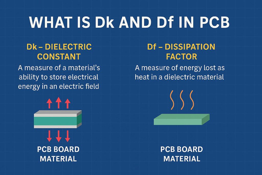
1. What is Dk in PCB?
Dk, or Dielectric Constant, also referred to as the Relative Permittivity (εr), is a measure of a material’s ability to store electrical energy in an electric field. It defines how much the material slows down an electric signal compared to the speed of light in a vacuum.
Key Points:
- Unitless value
- Higher Dk slows signal propagation
- Affects signal integrity and impedance
- Typical FR-4 Dk: 4.2 to 4.8 (depends on frequency and resin content)
In PCB design, consistent and known Dk values help engineers calculate trace impedance, which is crucial for impedance-controlled traces in high-speed circuits.
2. What is Df in PCB?
Df, or Dissipation Factor, is also known as the Loss Tangent or Tan δ. It quantifies the energy lost (as heat) due to the dielectric material when an AC signal passes through it.
Key Points:
- Measures energy loss in dielectric material
- Lower Df = better signal integrity
- Higher Df = more heat, more signal attenuation
- Typical Df for FR-4: 0.015 to 0.025
Df becomes particularly important as signal frequencies increase. In RF, microwave, and 5G systems, high Df can result in severe signal degradation.
3. Why Dk and Df Matter in PCB Design
As data rates increase, electromagnetic properties of PCB materials take center stage. Dk and Df directly affect:
- Signal Integrity: Mismatched or fluctuating Dk leads to reflections and distortions.
- Timing and Propagation Delay: Dk determines signal travel time across the board.
- Loss Budget: High Df consumes more of the signal’s power, reducing SNR (signal-to-noise ratio).
- Electromagnetic Interference (EMI): High Df can cause increased EMI due to heating and waveform distortion.
High-speed designers use simulation tools (like HyperLynx or Ansys SIwave) that factor in Dk and Df when predicting how a signal behaves across traces, vias, and planes.
4. Dk and Df Depend on Frequency
A major consideration is that Dk and Df are not constant across all frequencies. As the signal frequency increases:
- Dk tends to decrease slightly
- Df increases noticeably
Therefore, material suppliers often provide frequency-dependent Dk/Df values (e.g., measured at 1 GHz, 10 GHz, 40 GHz).
For example:
- FR-4 @ 1 GHz: Dk = 4.5, Df = 0.02
- Rogers RO4350B @ 10 GHz: Dk = 3.48, Df = 0.0037
This frequency dependence makes material selection critical for RF and high-speed digital designs like SerDes lanes, PCIe, and Ethernet.
5. Choosing the Right Material Based on Dk and Df
When selecting PCB laminate materials, the balance between performance, cost, and manufacturability is key. Here’s a general guide:
| Application | Recommended Material | Typical Dk | Typical Df |
| General Use | FR-4 | 4.4 | 0.02 |
| High-Speed Digital | Megtron 6, Isola I-Speed | 3.7–4.0 | 0.005–0.009 |
| RF / Microwave | Rogers RO4000 Series | ~3.5 | < 0.004 |
| 5G / mmWave | Rogers RT/Duroid, Tachyon | ~2.9–3.2 | < 0.0025 |
Keep in mind that as Df decreases, material cost tends to increase. For cost-sensitive products, trade-offs between performance and price must be carefully managed.
6. How Dk and Df Affect Impedance and Trace Geometry
Controlled impedance traces (like 50Ω or 100Ω differential pairs) are sensitive to Dk. To maintain impedance:
- Lower Dk = wider trace width required
- Higher Dk = narrower traces
For multilayer PCBs, trace width, spacing, and dielectric thickness must be adjusted based on the Dk of the material to maintain impedance.
Simulation and impedance calculators (like Polar Si9000) are used during layout to validate geometry against material properties.
7. Impact on Stack-up and PCB Layer Design
Stack-up planning involves selecting core and prepreg materials with suitable Dk/Df values. This is crucial for:
- Minimizing crosstalk
- Improving power integrity
- Ensuring signal delay consistency across layers
For example, a 10-layer PCB designed for high-speed networking must consider Dk variations layer by layer to ensure signal timing alignment across differential pairs.
8. Testing and Measuring Dk and Df
Material vendors use techniques like:
- Resonance Method
- Time Domain Reflectometry (TDR)
- Vector Network Analyzer (VNA) Testing
Designers often rely on vendor datasheets, but for critical designs, lab measurement or third-party testing may be required to ensure the values match expectations under real-world conditions.
9. Tips for Designers Working with Dk and Df
- Always use frequency-specific Dk/Df values in simulations.
- Watch for variation across batches of materials.
- Match materials across different board builds to ensure consistency.
- Validate impedance and loss budgets before finalizing the stack-up.
- Collaborate closely with your fabrication house to choose materials that meet both performance and manufacturability.
10. Final Thoughts: Why Dk and Df Define the Future of PCB Performance
With increasing demand for IoT, 5G, automotive radar, and cloud computing, signal integrity has never been more important. And at the heart of that integrity are material properties like Dk and Df.
Engineers must not only understand these parameters but design around them strategically, choosing materials and geometries that optimize performance while staying within manufacturing and budget constraints. Understanding What is Dk and Df in PCB equips designers with the insight to make smarter choices, minimize risk, and ensure robust performance in today’s demanding electronic systems.