
Printed Circuit Boards (PCBs) are the foundation of virtually all electronic devices. From simple gadgets to complex machinery, PCBs are crucial for ensuring electrical connections and the smooth functioning of components. PCB design services play a pivotal role in creating these essential components. In this article, we’ll explore various aspects of PCB design services, delving into each keyword to provide a detailed explanation.
What are PCB Design Services?
PCB design services encompass the entire process of creating a printed circuit board, from initial concept to final production. These services are crucial for translating electronic circuit designs into physical boards that can be used in devices. The key aspects of PCB design services include:
1. Custom PCB Design
Custom PCB design involves tailoring the PCB layout to meet specific requirements of a project. This customization ensures that the PCB fits perfectly within the intended device and functions as required. Customization may include specific shapes, sizes, or unique component placements to accommodate special features of the electronic device.
2. PCB Layout Design
PCB layout design is the process of arranging the components and routing the electrical connections on the board. A well-designed layout is essential for the efficient functioning of the PCB, minimizing signal interference and ensuring that the board can be manufactured effectively.
3. High-Speed PCB Design
High-speed PCB design is critical for applications that require rapid data transmission, such as in telecommunications and computing. These designs must consider factors like signal integrity and electromagnetic interference to ensure reliable performance at high speeds.
4. PCB Schematic Design
PCB schematic design is the blueprint of the circuit, showing how each component connects electrically. The schematic serves as a guide for creating the PCB layout, ensuring that the physical board matches the intended circuit functionality.
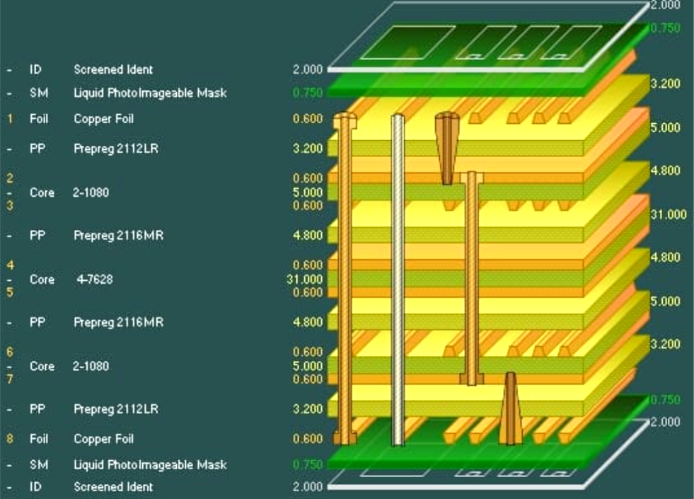
5. Multilayer PCB Design
Multilayer PCB design involves creating boards with multiple layers of circuitry. These designs are used in complex devices where space is limited, allowing for more compact and sophisticated electronic designs by stacking several layers of circuits.
6. PCB Prototyping Services
PCB prototyping services involve creating a small number of boards to test and validate a design before full-scale production. Prototyping is crucial for identifying and resolving issues early in the development process, saving time and costs in the long run.
7. PCB Manufacturing Services
PCB manufacturing services cover the production of the physical boards. These services ensure that the design specifications are met accurately, using advanced manufacturing techniques to produce reliable and high-quality PCBs.
8. PCB Assembly Services
PCB assembly services involve populating the board with electronic components. This process includes soldering components onto the PCB and ensuring that each part is correctly placed and connected, ready for use in electronic devices.
9. PCB Thermal Management
PCB thermal management is critical for maintaining the reliability and longevity of electronic devices. Effective thermal management solutions, such as heat sinks and thermal vias, help dissipate heat generated by components, preventing overheating and ensuring stable performance.
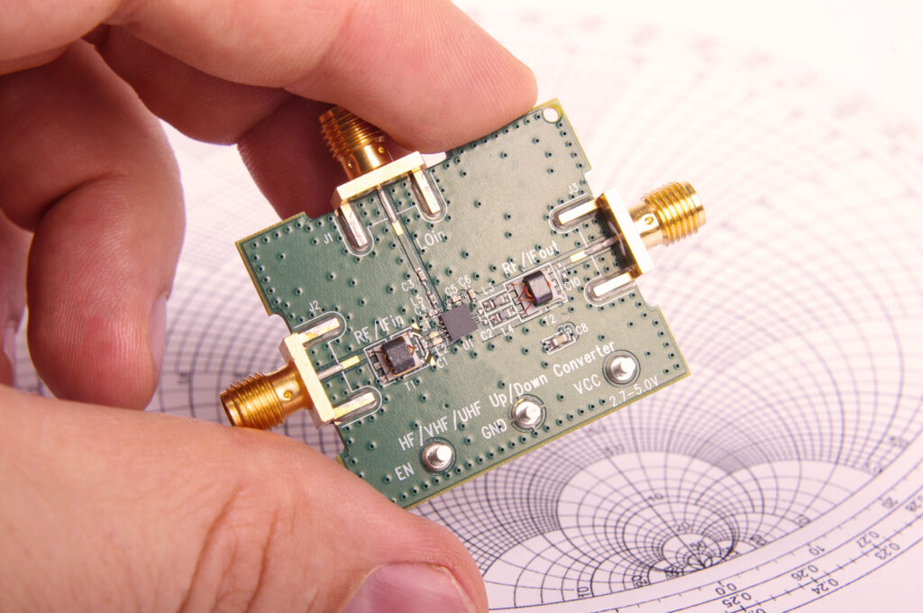
10. RF PCB Design
RF (Radio Frequency) PCB design focuses on circuits that operate at high frequencies. These designs require special considerations for signal integrity and impedance matching to ensure efficient transmission of radio signals without interference.
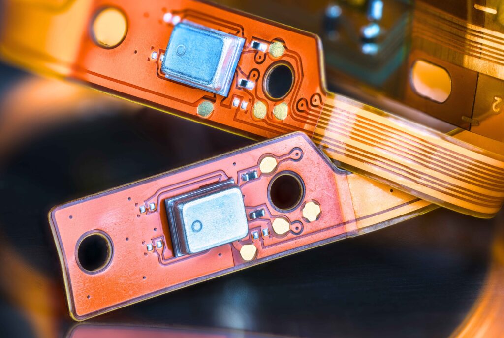
11. Flexible PCB Design
Flexible PCB design involves creating boards that can bend and flex without breaking. These designs are used in applications where space is limited or where the board needs to conform to a specific shape, such as in wearable electronics and flexible displays.
12. PCB CAD Design
PCB CAD (Computer-Aided Design) design utilizes software tools to create and visualize PCB layouts. CAD tools allow designers to create precise and complex designs, simulate circuit behavior, and optimize the layout before manufacturing.
13. PCB Design for Manufacturing
PCB design for manufacturing (DFM) ensures that the PCB design is optimized for efficient production. DFM considerations include ease of assembly, material selection, and minimizing potential manufacturing defects, ensuring a smooth transition from design to production.
14. PCB Signal Integrity Analysis
PCB signal integrity analysis involves examining the PCB layout to ensure that signals are transmitted without distortion or loss. This analysis is crucial for high-speed and high-frequency designs, where maintaining signal quality is essential for proper functioning.
15. PCB Design Guidelines
PCB design guidelines provide best practices for creating effective and reliable PCBs. These guidelines cover various aspects, such as component placement, routing techniques, and material selection, helping designers create high-quality boards that meet industry standards. Usually, these guidelines come with a checklist at the end that helps the designer to assure the quality of the PCB and all necessary considerations in the design.
16. PCB Design Optimization
PCB design optimization focuses on improving the design to enhance performance, reduce costs, and ensure manufacturability. Optimization techniques may include refining the layout, selecting appropriate materials, and minimizing unnecessary components. Usually in larger companies a team will review each design and they come back with a list of optimizations before the design gets frozen.
17. PCB Design and Testing
PCB design and testing involve validating the design through various tests to ensure it meets the required specifications. Testing can include functional tests, signal integrity tests, and thermal analysis, identifying and resolving issues before mass production. One of the basic tests after production is a flying probe test that assures the connectivity between each net point and it can be up to 100% of all connections.
18. PCB Design Consultation
PCB design consultation services provide expert advice and guidance throughout the design process. Consultants can help with design reviews, optimization strategies, and troubleshooting, ensuring that the final design meets the project requirements. This consultation can save the project a lot of time and money as a mistake in PCB design will push the project schedule back for a long time and obviously remaking the PCB needs extra funds. Arshon Technology is happy to help anyone who is interested in consulting services.
19. PCB Reverse Engineering
PCB reverse engineering involves analyzing an existing PCB to understand its design and functionality. This process can be used to replicate or improve a design, especially when original documentation is unavailable. PCB reverse engineering can be a difficult task especially when the number of layers is more than two. When you deal with a 6-layer or 8-layer PCB, reverse engineering may need delamination of the PCB and a lot of hours of engineering work. The possibility of error is also very high in this tedious work.
20. PCB Design Review
PCB design review is a critical step in the design process, involving a thorough examination of the layout to identify potential issues. Design reviews help ensure that the PCB meets all requirements and is free of errors before production. The best person to review the PCB is the PCB manufacturing expert, who understands the process of manufacturing and can catch the issues before your board gets into the process of being built.
21. PCB Component Placement
PCB component placement is the strategic arrangement of electronic components on the board. Proper placement is crucial for optimal performance, signal integrity, and ease of assembly. Therefore, the PCB designer’s first task is to place the components on the board and make sure the electrical routing is minimum between the parts, before starting the routing process. For example, if there are many electrical connections between two parts and these two are on the two sides of the board, there will be a lot of traces extended from one side of the PCB to the other side, which is not good design.
22. PCB Power Integrity
PCB power integrity ensures that the board can deliver stable and reliable power to all components. This involves careful design of power distribution networks and minimizing noise and voltage drops.
PCB (Printed Circuit Board) power integrity refers to the ability of a circuit board to deliver stable and reliable power to all components under varying operational conditions. It’s a critical aspect of electronic design, ensuring that voltage and current supply meet the requirements of sensitive components without introducing noise or fluctuations that could degrade performance or cause malfunction.
PCB power integrity considerations are crucial in high-speed digital designs, RF circuits, and any application where stable power delivery is paramount for reliable performance and longevity of electronic devices. By implementing these principles, designers can mitigate risks associated with power-related issues and ensure the overall robustness of their electronic systems.
23. PCB Design Documentation
PCB design documentation provides detailed information about the PCB design, including schematics, layout files, and manufacturing instructions. Comprehensive documentation is essential for ensuring accurate production and facilitating future maintenance or modifications.
Typically, these documents express the material type, thickness of PCB, type of finish, thickness of copper, number of layers and thickness of each layer.
24. PCB Design Software Tools
PCB design software tools are essential for creating, simulating, and optimizing PCB layouts. These tools provide powerful features for schematic capture, layout design, and signal integrity analysis, streamlining the design process. Some famous software tools are Cadence, Allegro, Altium and Eagle PCB.
25. PCB Design Services: Bringing It All Together
PCB design services are indispensable for creating the complex electronic boards that power modern devices. From custom designs to high-speed applications, and from prototyping to full-scale manufacturing, these services cover every aspect of PCB creation. By leveraging advanced software tools, adhering to best practices, and ensuring thorough testing, PCB design services deliver high-quality, reliable boards that meet the specific needs of each project.
Conclusion
The world of PCB design services is vast and multifaceted, encompassing a wide range of skills and technologies. Understanding each aspect, from custom PCB design and layout to signal integrity analysis and thermal management, is crucial for creating effective and reliable PCBs. Whether you’re working on a simple gadget or a complex industrial system, PCB design services provide the expertise and tools needed to bring your electronic designs to life.
By adhering to industry guidelines, optimizing designs for performance and manufacturability, and ensuring thorough testing and documentation, PCB design services ensure that every board meets the highest standards of quality and functionality. As technology continues to evolve, the role of PCB design services will remain pivotal, driving innovation and enabling the development of the next generation of electronic devices.