
Printed Circuit Boards (PCBs) are integral to the functionality of virtually all electronic devices, from household gadgets to advanced aerospace technology. However, designing PCBs for underwater applications presents a unique set of challenges that require specialized knowledge, materials, and manufacturing techniques. This article explores the intricacies of underwater PCB design, focusing on PCB fabrication, PCB manufacturing processes, electronic design considerations, and material selection, while addressing the distinct environmental challenges of underwater environments.
Underwater PCB Design
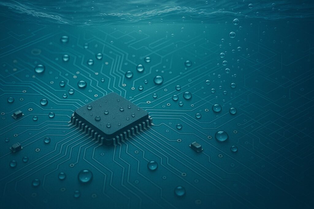
Underwater PCB design involves creating electronic circuits capable of operating reliably in submerged or marine environments. This field includes applications like underwater drones (ROVs and AUVs), marine monitoring systems, submarine electronics, underwater communication systems, and equipment for offshore oil and gas exploration. The primary goal of underwater PCB design is ensuring long-term reliability, functionality, and resistance to environmental stresses, particularly moisture ingress, pressure extremes, and corrosive seawater.
Applications of PCBs in Underwater Environments
PCBs designed for underwater applications find their homes in various industries and devices, including:
- Marine Technology: Underwater robots, autonomous underwater vehicles (AUVs), and remotely operated vehicles (ROVs) benefit from specialized PCBs that help with navigation, data collection, and communication measures.
- Submersibles: Deep-sea exploration and research submersibles rely on complex electronics contained within PCBs to operate sensors, cameras, and scientific instruments at great depths.
- Oceanographic Instruments: Scientific research devices that monitor water quality, temperature, and currents utilize PCBs to transmit crucial data while subjected to perilous conditions.
- Environmental Monitoring: Sensors for monitoring underwater ecosystems and marine life also benefit from tailored PCB designs that protect against corrosion and water damage.
Unique Challenges in PCB Design for Underwater Applications
Designing PCBs for underwater environments introduces several unique challenges:
- Water Ingress and Moisture: Continuous exposure to moisture is one of the greatest threats, potentially causing short circuits, corrosion, and reliability issues.
- Pressure Extremes: Underwater systems often operate at high pressures, requiring designs capable of resisting structural deformation.
- Corrosion: Seawater, with its high salinity and chemical makeup, accelerates corrosion and deterioration of metals and solder joints.
- Temperature Variation: Underwater electronics can experience rapid temperature changes, necessitating robust thermal management.
- Electrical Isolation: Maintaining electrical isolation and insulation is critical due to the conductive nature of water.
- Signal Integrity: Ensuring signal quality despite water interference and attenuation requires careful consideration during design.
Reliability Concerns in Extreme Environments
The extreme conditions associated with underwater applications raise significant reliability concerns. Circuit boards must function reliably over extended periods, even under high pressure and corrosive conditions. A failure in any component can lead to catastrophic consequences, making the design and selection of materials critical. Engineers must prioritize redundancy, robust design, and thorough testing to ensure that the PCB can withstand extreme environments and continue to function as intended.
Materials and Coatings
Selecting the appropriate materials and protective coatings is crucial in underwater PCB design to combat environmental challenges:
Substrate Materials
- FR-4: Standard PCB substrate, affordable but limited in thermal conductivity and water resistance.
- Polyimide: Superior flexibility, heat resistance, and durability, making it ideal for rugged underwater environments.
- Ceramic and Metal-Core PCBs: Excellent thermal dissipation and structural integrity, suitable for high-pressure deep-water applications.
Protective Coatings
- Conformal Coating: Polyurethane, silicone, acrylic, or epoxy-based coatings applied directly to PCBs to protect from moisture and corrosion.
- Potting Compounds: Epoxy or silicone encapsulation provides a robust moisture barrier and additional mechanical support.
- Parylene Coating: Thin-film polymer offering outstanding waterproofing and chemical resistance.
Benefits of Using Specialized Materials and Their Impact on Performance
Utilizing specialized materials and coatings results in improved performance and extends the lifespan of the PCB. Enhanced resistance to corrosion and moisture intrusion minimizes failure rates, while specific formulations can target the distinct challenges posed by underwater environments. The right combination of materials ensures that devices remain operational amidst harsh conditions, ultimately reducing long-term costs associated with repairs and replacements.
Design Considerations
Underwater PCB design must integrate critical design considerations that address environmental impacts:
- Seal Integrity: Ensuring all electronic enclosures are hermetically sealed to prevent moisture ingress.
- Component Selection: Using components specifically rated for harsh environments, ensuring reliability under pressure and exposure.
- Thermal Management: Effective heat dissipation through thermal vias, heat sinks, and advanced substrate materials.
- Trace Width and Spacing: Enhanced trace spacing and thick copper layers to prevent shorts from moisture and enhance signal integrity.
- EMI/EMC Considerations: Incorporating shielding and grounding strategies to mitigate electromagnetic interference (EMI).
- Pressure Management: Structural design considerations to withstand high pressures without deformation or damage.
Manufacturing Techniques
The manufacturing of PCBs for underwater applications involves specialized processes that account for extreme conditions. Techniques may include:
- High-Density Interconnect (HDI): HDI technology allows for more miniaturized designs, which is particularly beneficial in compact underwater devices.
- Via-in-Pad Technology: This approach can provide enhanced reliability and thermal management in tight layouts, allowing components to be placed even more closely together.
Tolerance and Quality Control Measures to Ensure Reliability in Harsh Conditions
Quality control is paramount in the manufacturing of underwater PCBs. Techniques include:
- Automated Optical Inspection (AOI): Rigorous inspections ensure that every board meets specifications before leaving the manufacturing facility.
- Functional Testing: Each completed PCB should undergo functional testing to confirm electrical performance, which is critical in high-stakes underwater applications.
Exploration of Advanced Techniques, Such as 3D Printing for Prototypes
3D printing and other advanced manufacturing techniques are becoming increasingly popular for PCB prototyping. Benefits include:
- Rapid Prototyping: Quick iterations allow for faster development cycles, enabling designers to test concepts thoroughly before moving into full-scale production.
- Complex Geometries: 3D printing can create unique shapes and features, facilitating designs that traditional PCB manufacturing may not easily allow.
Case Studies
Case Study 1: Autonomous Underwater Vehicles (AUVs)
AUV electronics must withstand high pressures and corrosion. A successful design incorporated ceramic substrates with epoxy potting to ensure long-term reliability. Thermal management was achieved via metal-core substrates, dramatically improving the operational lifespan and minimizing maintenance requirements.
Case Study 2: Marine Sensor Networks
Marine sensor network nodes require durable and corrosion-resistant PCBs. Engineers employed polyimide substrates with parylene conformal coating, dramatically enhancing moisture resistance. Enhanced EMI shielding ensured clear communication despite environmental interference, significantly increasing the system’s reliability.
Case Study 3: Deep-Sea Exploration Equipment
For deep-sea exploration gear, traditional FR-4 substrates were replaced with metal-core PCBs and ceramic materials to withstand extreme pressures. A dual-layer protective coating (conformal coating plus potting compound) provided comprehensive environmental protection. Rigorous testing validated designs capable of operating reliably at ocean depths exceeding 6000 meters.
Lessons Learned from Each Case and How Challenges Were Overcome
From these examples, key lessons include:
- Material Selection Matters: Choosing the right materials affects the lifespan and reliability of underwater devices significantly.
- Prototyping is Crucial: Rigorous testing and prototyping can reveal unforeseen issues, enabling faster troubleshooting and design improvements.
Notable Examples from Industries Like Marine Exploration, Robotics, or Environmental Monitoring
The shift toward more robust materials and innovative designs in the marine sector, especially in environmental monitoring, reflects the growing need for sustainable practices. For instance, initiatives utilizing underwater drones equipped with specialized PCBs are aiding conservation efforts, measured through accurate data collection on marine ecosystems.
By integrating advanced technology, these industries can enhance their impact through actionable data while mitigating risks associated with traditional sensors.
Conclusion
PCB design for underwater applications demands meticulous attention to materials, protective coatings, manufacturing techniques, and specialized design considerations to mitigate environmental impacts. Leveraging advanced electronic design practices ensures robust performance and long-term reliability, even in the most demanding underwater conditions. The continuous evolution in PCB fabrication and manufacturing technologies further enhances the resilience and functionality of underwater electronic systems, providing reliable solutions for marine, subsea, and deep-ocean applications.