
The world of electronics owes much of its advancement to the development of Printed Circuit Boards (PCBs), and at the core of every PCB lies the Copper Clad Laminate (CCL). This material serves as the foundational layer for PCB manufacturing, providing the structural support and conductive pathways necessary for electronic devices to function. This article explores the essential aspects of copper clad laminates, their types, properties, and significance in PCB design and PCB prototyping.
What is Copper Clad Laminate?
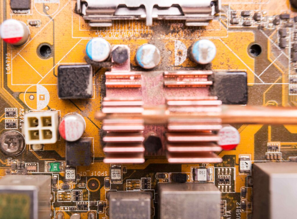
A Copper Clad Laminate (CCL) is a composite material made by bonding a thin layer of copper foil to a substrate, typically made of insulating materials like fiberglass or resin. These laminates form the base of PCBs, where the copper layers are etched to create conductive pathways.
Composition of Copper Clad Laminates
The performance and quality of a CCL depend on its composition, which generally includes:
- Copper Foil: Acts as the conductive layer. The thickness of the copper can vary, depending on the application.
- Substrate: Provides mechanical support and insulation. Common materials include:
- FR4 (fiberglass reinforced epoxy): The most widely used substrate due to its excellent thermal and electrical properties.
- Polyimide: Used in flexible PCBs due to its flexibility and heat resistance.
- Ceramic: Preferred for high-frequency applications due to low dielectric losses.
- Adhesive Layer: Bonds the copper foil to the substrate, often made of resin or other bonding agents.
Types of Copper Clad Laminates
CCLs come in various types to suit different applications. Key classifications include:
1. Based on Material:
- FR4 Laminate: The industry standard for general-purpose PCBs.
- Flexible CCLs: Made with polyimide substrates for flexible circuits.
- Metal Core CCLs: Feature a metal core for improved heat dissipation in power electronics.
2. Based on Copper Thickness:
- Standard Copper (1 oz/ft²): Suitable for most electronic applications.
- Heavy Copper (>2 oz/ft²): Used in high-current or power applications.
3. Based on Application:
- High-Frequency CCLs: Designed for RF and microwave circuits.
- High-Thermal CCLs: Used in applications requiring excellent thermal management.
Properties of Copper Clad Laminates
Understanding the properties of CCLs is crucial in PCB design and PCB prototyping. These include:
1. Mechanical Properties
- Tensile Strength: Ensures durability during handling and assembly.
- Flexural Strength: Important for flexible or multilayer PCBs.
2. Thermal Properties
- Glass Transition Temperature (Tg): Indicates the temperature at which the material transitions from rigid to soft.
- Thermal Conductivity: Key for heat dissipation in high-power circuits.
3. Electrical Properties
- Dielectric Constant (Dk): Determines signal propagation speed.
- Dissipation Factor (Df): Indicates energy loss in high-frequency applications.
4. Chemical Properties
Flame Resistance: Many CCLs meet UL94-V0 standards for fire safety.
Moisture Absorption: Low absorption is critical for reliability in humid environments.
Role of Copper Clad Laminates in PCB Design
Copper clad laminates play a pivotal role in PCB design, influencing both performance and manufacturability. Key considerations include:
- Substrate Selection: Choosing the right material for thermal, mechanical, and electrical requirements.
- Copper Thickness: Ensuring adequate current-carrying capacity while avoiding excessive weight or cost.
- Layer Count: Determining single-layer, double-layer, or multilayer designs based on complexity.
- Surface Finish Compatibility: Ensuring the CCL is compatible with surface finishes like HASL, ENIG, or OSP.
Copper Clad Laminates and PCB Prototyping
During the PCB prototyping phase, CCLs are essential for evaluating designs and materials. Prototyping often involves:
- Material Testing: Assessing the performance of different substrates and copper thicknesses.
- Signal Integrity Testing: Ensuring low dielectric losses for high-frequency applications.
- Thermal Testing: Verifying heat dissipation for power-intensive designs.
Prototyping with high-quality CCLs helps identify potential issues early, reducing costs and ensuring a smoother transition to mass production.
Challenges in Using Copper Clad Laminates
Despite their versatility, CCLs present some challenges:
- Warpage: Improper handling or processing can lead to bending, affecting PCB quality.
- Delamination: Poor bonding between copper and substrate can cause separation.
- Environmental Concerns: Disposal and recycling of CCLs require adherence to environmental regulations.
Mitigating these issues involves careful material selection, process optimization, and compliance with standards like RoHS.
Advances in Copper Clad Laminates
The demand for more compact, high-performance electronics has driven innovations in CCL technology. Recent developments include:
- Halogen-Free Laminates: Environmentally friendly options that meet strict safety standards.
- Ultra-Thin Laminates: Ideal for miniaturized devices.
- High-Speed Materials: Designed for 5G and other high-frequency applications.
Conclusion
Copper Clad Laminates are the backbone of PCB manufacturing, providing the essential structure and properties required for modern electronic devices. Their versatility and adaptability make them suitable for a wide range of applications, from consumer electronics to advanced aerospace systems.
By understanding the types, properties, and challenges of CCLs, designers and manufacturers can make informed choices that enhance performance and reliability. Whether in PCB design, PCB prototyping, or mass production, the importance of copper clad laminates cannot be overstated, as they lay the foundation for innovation in the electronics industry.