
Introduction
In the vast world of electronics, Printed Circuit Boards (PCBs) stand as the backbone of modern devices. They interconnect and support components, enabling everything from simple LED circuits to complex automotive control systems. Among the many types of PCBs, Single Layer PCB (also known as “single-sided PCB”) is the simplest form. As consumer demand varies and technologies evolve, single-layer boards remain relevant for a host of applications due to their low cost, quick turnaround time, and ease of fabrication.
This extensive guide will walk you through the fundamentals of Single Layer PCB Design, focusing on essential aspects like stackups, manufacturing processes, design examples, software, and best practices. We’ll also explore the advantages, disadvantages, and use cases of single-sided PCBs. Finally, we’ll highlight how Arshon Technology supports organizations by providing premium PCB Design and PCB Manufacturing services.
What Is a Single Layer PCB?
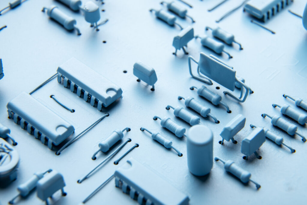
A Single Layer PCB or single-sided PCB has only one conductive copper layer. Components are typically placed on one side of the board, and the copper traces that connect the components are etched or printed on the same side. This type of PCB is popular for simpler, cost-effective electronic solutions—like LED circuits, household appliances, or basic sensors—where high-density component placement and complex routing are not required.
Key Features of Single-Sided PCBs
- Only one copper layer for routing.
- No plated-through holes (via-holes can exist but are often non-plated or rarely needed).
- Simpler layout and design compared to double-sided and multilayer PCBs.
- Lower manufacturing costs due to reduced material usage and processing steps.
Single Layer PCB Design Example
To illustrate the concept, let’s consider a basic LED controller as a straightforward Single Layer PCB Design example:
- Power Source: A simple 5V supply or a battery.
- LED: A light-emitting diode (the main output device).
- Resistor: To limit current through the LED.
- Switch or Transistor: To turn the LED on and off.
- Miscellaneous Components: Possibly a small capacitor for noise filtering.
Design Approach:
- Place the power connector and LED in a position convenient for the product enclosure.
- Include a resistor in series with the LED to set the appropriate current.
- Mount a small transistor and a switch if the design must toggle the LED electronically.
- Route copper traces on the same side where components are mounted.
In practice, this entire circuitry might require only a few square centimeters of board real estate. The single conductive layer simplifies manufacturing, and minimal drilling is needed—making it ideal for rapid prototyping and high-volume production alike.
Single Layer PCB Design Template
A Single Layer PCB Design Template acts as a starting framework that engineers or hobbyists can reuse across multiple projects. Such templates often include:
- Board Outline
A standard shape and dimension (e.g., 50 mm x 50 mm) or a form tailored to product enclosures. - Mounting Holes
Predefined positions for screws or standoffs if the board is part of a larger assembly. - Generic Component Footprints
For instance, standard footprints for resistors (0805 or 1206), capacitors, and popular integrated circuits. - Silkscreen Layer and Labels
A consistent style for labeling components (e.g., “R1” for resistors, “C1” for capacitors). - Pre-Routed Power Lines
Some templates include pre-designed power distribution areas or copper pours to simplify design.
Why Use a Template?
- Time-Saving: Reuse instead of redesign from scratch.
- Consistency: Ensures uniform board appearance and assembly process.
- Reduction in Errors: Minimizes risk of spacing or footprint mistakes.
Single Layer PCB Design Software
The PCB Design ecosystem is broad, with software ranging from beginner-friendly tools to professional suites. Below are some popular options well-suited for Single Layer PCB projects:
- KiCad
- Cost: Free, open-source.
- Features: Schematic capture, PCB layout, 3D board visualization, advanced libraries.
- Pros: Large community support, no licensing constraints, frequent updates.
- Cost: Free, open-source.
- Eagle PCB
- Cost: Subscription-based, with a free tier for small boards.
- Features: Schematic editor, auto-routing, large library ecosystem.
- Pros: Widely known and documented, integrates with Fusion 360 for mechanical design.
- Cost: Subscription-based, with a free tier for small boards.
- EasyEDA
- Cost: Free, browser-based.
- Features: Online schematic and PCB editor, cloud libraries, direct ordering from JLCPCB.
- Pros: No local installation needed, ideal for quick collaborative projects.
- Cost: Free, browser-based.
- Altium Designer
- Cost: Premium software with licensing fees.
- Features: High-level schematic and PCB tools, 3D visualization, advanced simulation, large library integration.
- Pros: Industry-standard for complex designs, robust collaboration features.
- Cost: Premium software with licensing fees.
- Fritzing
- Cost: Low one-time cost or donation-based model.
- Features: Breadboard view, schematic view, PCB layout.
- Pros: Beginner-focused, interactive interface, widely used in educational settings.
- Cost: Low one-time cost or donation-based model.
Choosing Software depends on project complexity, budget, personal preference, and collaboration needs. For simple boards, even free software can handle all necessary tasks from schematic creation to Gerber file export.
How to Design a Single-Layer PCB?
Designing a Single Layer PCB follows a logical workflow that ensures the resulting board meets electrical and mechanical requirements:
- Schematic Capture
- Draw your circuit in a schematic editor, assigning each component a specific reference designation (R1, C1, U1, etc.).
- Use a netlist to define electrical connections between components.
- Draw your circuit in a schematic editor, assigning each component a specific reference designation (R1, C1, U1, etc.).
- Footprint Assignment
- Map each schematic symbol to the correct PCB footprint (e.g., an 0805 resistor, TO-92 transistor).
- Verify pad sizes and hole diameters meet manufacturing tolerances.
- Map each schematic symbol to the correct PCB footprint (e.g., an 0805 resistor, TO-92 transistor).
- Initial Board Setup
- Create or select a Single Layer PCB Design template.
- Define board dimensions and shape.
- Create or select a Single Layer PCB Design template.
- Component Placement
- Place critical components first (e.g., microcontrollers, connectors).
- Group related components to minimize trace lengths and reduce EMI.
- Place critical components first (e.g., microcontrollers, connectors).
- Trace Routing
- Since there’s only one copper layer, plan your paths carefully.
- Maintain adequate spacing between traces to prevent shorts.
- If crossing traces is unavoidable, consider jumpers or zero-ohm resistors (though rarely used in single-layer designs).
- Since there’s only one copper layer, plan your paths carefully.
- Add Silkscreen Labels
- Label part references and orientations.
- Place text away from drill holes and pads to ensure readability.
- Label part references and orientations.
- Design Rule Checks (DRC)
- Tools automatically check trace widths, spacing, and pad connections.
- Resolve errors (short circuits, clearance issues) before finalizing.
- Tools automatically check trace widths, spacing, and pad connections.
- Gerber File Generation
- Export final layout into Gerber format.
- Generate drill files, solder mask, and silkscreen layers as needed.
- Export final layout into Gerber format.
- Prototype or Final Manufacture
- Send Gerbers to a PCB Manufacturer for production.
- Double-check all design specifics (copper thickness, substrate materials, finish, etc.).
- Send Gerbers to a PCB Manufacturer for production.
By following these steps methodically, errors are minimized, and production often goes smoothly.
Single Layer PCB Stackup
Whereas multi-layer boards may have complex internal structures with multiple layers of copper, Single Layer PCB Stackup is far more straightforward:
- Silkscreen Layer (Top):
- This optional layer shows component outlines and references.
- This optional layer shows component outlines and references.
- Solder Mask (Top):
- A protective polymer layer that covers copper traces and pads.
- Only the holes or pads that need soldering are exposed.
- A protective polymer layer that covers copper traces and pads.
- Copper Layer:
- The sole conductive layer for routing and component pads.
- Copper thickness is typically 1 oz/ft² (~35 µm) for most commercial boards but can vary (0.5 oz to 4 oz or more).
- The sole conductive layer for routing and component pads.
- Substrate (Base Material):
- The insulating platform (usually FR-4).
- Occasionally, less expensive materials like phenolic or CEM may be used for very low-cost applications.
- The insulating platform (usually FR-4).
Some manufacturers may refer to the top side as the “component side” and the copper side as the “foil side.” However, in many single-sided boards, the copper side is also where components might be soldered through the board from the “top” (depending on orientation).
Single Layer PCB Manufacturing Process
The PCB Manufacturing flow for single-sided boards can be summarized in these steps:
- Material Preparation
- The manufacturer starts with a copper-clad laminate (FR-4 or another substrate).
- The copper thickness is chosen based on design requirements (1 oz/ft² is standard).
- The manufacturer starts with a copper-clad laminate (FR-4 or another substrate).
- Photoresist Application
- The copper surface is coated with a photo-sensitive film.
- This resist will be removed in areas where copper must be etched away.
- The copper surface is coated with a photo-sensitive film.
- Image Transfer
- An artwork film (generated from the Gerber files) is placed over the board.
- Ultraviolet (UV) light exposure hardens the resist in the areas where copper must remain.
- An artwork film (generated from the Gerber files) is placed over the board.
- Development
- Unexposed resist (where traces are not needed) is washed away, leaving only the copper traces protected by the hardened resist.
- Unexposed resist (where traces are not needed) is washed away, leaving only the copper traces protected by the hardened resist.
- Etching
- The board is submerged in an acid or alkaline solution that dissolves the exposed copper, forming the desired traces.
- The board is submerged in an acid or alkaline solution that dissolves the exposed copper, forming the desired traces.
- Strip the Resist
- The remaining photoresist, protecting the traces, is removed, revealing the final copper pattern.
- The remaining photoresist, protecting the traces, is removed, revealing the final copper pattern.
- Solder Mask Application (If needed)
- A green (or other color) epoxy mask is applied to protect the copper traces.
- Openings are made for component pads or through-holes.
- A green (or other color) epoxy mask is applied to protect the copper traces.
- Silkscreen Printing (Optional)
- Text and component outlines are added on top of the solder mask.
- Text and component outlines are added on top of the solder mask.
- Drilling and Profiling
- If holes or board outlines are required, these are machined to specified dimensions.
- If holes or board outlines are required, these are machined to specified dimensions.
- Surface Finishing
- Surfaces exposed for soldering may receive finishes like HASL (Hot Air Solder Leveling), ENIG (Electroless Nickel Immersion Gold), or OSP (Organic Solderability Preservative).
- Quality Control
- Automated optical inspection (AOI), electrical tests, and visual checks ensure the board meets specs.
Given the relative simplicity of single-sided boards, these steps are performed quickly and at a lower cost than more complex multilayer processes.
What Are the Characteristics of Single-Layer PCB?
The defining attributes of Single Layer PCB (or single-sided PCB) include:
- Cost-Effectiveness
- Requires fewer materials (only one copper layer).
- Lower per-board cost, especially for high-volume runs.
- Requires fewer materials (only one copper layer).
- Simplified Design
- Reduces the time and complexity of routing.
- Ideal for straightforward or lower-density circuits.
- Reduces the time and complexity of routing.
- Faster Turnaround
- Fewer fabrication steps and simpler QC procedures.
- Short lead times for prototypes and mass production.
- Fewer fabrication steps and simpler QC procedures.
- Lower Thermal Dissipation Capabilities
- With only one copper plane, heat spreading is less efficient compared to multi-layer boards with dedicated ground or power planes.
- With only one copper plane, heat spreading is less efficient compared to multi-layer boards with dedicated ground or power planes.
- Limited Routing Space
- Only one layer for all traces—makes advanced or high-pin-count designs challenging.
- Only one layer for all traces—makes advanced or high-pin-count designs challenging.
- Straightforward Assembly
- Components placed on top, soldered onto that same side, or placed through holes if needed.
- Components placed on top, soldered onto that same side, or placed through holes if needed.
Overall, single-sided boards are designed for applications that do not demand extremely high component density or advanced features like impedance control or sophisticated power distribution.
What Are the Disadvantages of Single-Sided PCB?
Despite their advantages, single-sided boards do have drawbacks:
- Limited Routing
- Having just one layer severely restricts the ability to route complex circuits.
- Having just one layer severely restricts the ability to route complex circuits.
- Higher EMI Susceptibility
- Lack of dedicated ground planes can lead to increased electromagnetic interference, especially at high frequencies.
- Lack of dedicated ground planes can lead to increased electromagnetic interference, especially at high frequencies.
- Lower Component Density
- Large or complex circuits often require multi-layer solutions to fit everything on a reasonable footprint.
- Large or complex circuits often require multi-layer solutions to fit everything on a reasonable footprint.
- Increased Board Size
- More space is necessary for trace routing. Components may be spread out, leading to bigger boards.
- More space is necessary for trace routing. Components may be spread out, leading to bigger boards.
- No True Separation of Power and Ground
- Multi-layer boards often benefit from at least one full ground plane, improving signal integrity and noise performance.
- Multi-layer boards often benefit from at least one full ground plane, improving signal integrity and noise performance.
When the design constraints surpass the capabilities of a single-sided board, engineers often opt for double-sided or multi-layer PCBs despite the higher costs.
Why Are Single-Sided PCBs Used?
Given these disadvantages, you might wonder why single-sided PCBs are still so popular. The reasons are straightforward:
- Economical for Mass Production
- A single copper layer and simpler fabrication steps translate to budget-friendly production, especially in large volumes.
- A single copper layer and simpler fabrication steps translate to budget-friendly production, especially in large volumes.
- Simplicity is an Asset
- For many consumer goods, toys, and home appliances, the circuit is not complex enough to necessitate multiple layers.
- For many consumer goods, toys, and home appliances, the circuit is not complex enough to necessitate multiple layers.
- Fast Prototyping
- Rapid iteration is possible since single-sided boards have a short turnaround time.
- Rapid iteration is possible since single-sided boards have a short turnaround time.
- Lower-Risk Design
- Fewer layers mean fewer opportunities for manufacturing defects, such as misaligned vias or layer registration errors.
- Fewer layers mean fewer opportunities for manufacturing defects, such as misaligned vias or layer registration errors.
- Educational Value
- Single layer PCBs are often the first boards electronics students or hobbyists learn to design, thanks to their minimal complexity.
- Single layer PCBs are often the first boards electronics students or hobbyists learn to design, thanks to their minimal complexity.
In many scenarios, single-sided solutions strike an optimal balance between functionality, cost, and ease of production.
Related Considerations: When to Move Beyond Single Layer
While Single Layer PCB Design is indeed cost-effective, there are cases where upgrading to double-sided or multi-layer boards is essential:
- High-Speed Signals: Requires ground planes and controlled impedance routing.
- Compact Footprint: Multiple layers help pack dense circuits into smaller spaces.
- Advanced Thermal Management: Additional copper planes and thermal vias improve heat dissipation.
- EMC/EMI Constraints: Dedicated ground planes reduce noise and interference.
- Power Integrity: Planes for power distribution help stabilize supply lines in complex designs.
These factors often push engineers to select a more advanced approach, but for simpler electronic systems, single-sided remains compelling.
Arshon Technology: Your Partner in PCB Design and Manufacturing
When it comes to PCB Design and PCB Manufacturing, partnering with the right service provider can mean the difference between a product that faces delays and quality issues, and one that seamlessly enters the market. Arshon Technology specializes in delivering top-notch Single Layer PCB and multi-layer boards for an array of industries.
Our experts leverage industry-leading tools and technologies to ensure each project is optimized for performance, manufacturability, and cost. Whether you’re seeking a simple single-sided board for a basic consumer device or a complex multi-layer solution for high-speed data processing, our team’s commitment to quality, rapid turnaround, and rigorous testing guarantees a seamless path from concept to final product.

Key Advantages of Working with Arshon Technology:
- Comprehensive Support: From schematic capture and layout to final fabrication and assembly.
- ISO-Certified Quality: Ensuring every board meets or exceeds industry standards.
- Flexibility: Projects range from small prototypes to large production runs.
- Cutting-Edge Tools: We maintain up-to-date software and equipment, supporting advanced design features.
- Dedicated Team: Our engineers and technicians are well-versed in a range of verticals, ensuring domain-specific insight.
By entrusting your Single Layer PCB or more complex needs to Arshon Technology, you’re securing a manufacturing partner that values precision, reliability, and continuous innovation.
Conclusion
Single Layer PCB Design might be the simplest form of PCB engineering, but it remains deeply relevant in today’s electronics landscape. From educational kits and prototypes to mass-produced appliances and low-power products, the single-sided approach offers unmatched cost efficiency and speed.
Designing a single-sided board involves a deliberate approach—balancing component placement, routing, and manufacturing limitations. While single-layer PCBs aren’t suitable for high-density, high-speed applications, they offer a streamlined solution for countless consumer and industrial projects. Their straightforward stackup, well-established manufacturing processes, and quick turnaround times are particularly attractive to small businesses, hobbyists, and large-scale manufacturers aiming to keep costs low.
Moreover, having a trusted partner like Arshon Technology can elevate the design-to-production journey, ensuring each board is meticulously planned, fabricated, and tested to meet the highest standards. Whether you’re beginning your PCB design journey or refining an existing product, a robust understanding of single-layer concepts is foundational in the broader realm of PCB Design and PCB Manufacturing.