
As technological innovation accelerates, PCB Design, PCB Fabrication, and PCB Manufacturing continue to drive advancements in virtually every sector—from consumer electronics to medical devices and industrial automation. However, with the growing reliance on electronic products, it’s critical to consider the environmental and health impacts associated with PCB hazardous material. Printed Circuit Boards (PCBs), while essential components of modern electronic devices, are often composed of materials that can pose risks if not properly handled during manufacturing, use, and end-of-life disposal.
This comprehensive guide explores PCB hazardous material, detailing what substances are considered hazardous, their implications for human health and the environment, and how the PCB manufacturing industry is adapting through safer practices, compliance standards, and eco-friendly innovations.
What Is PCB Hazardous Material?
PCB hazardous material refers to substances used in the PCB fabrication process or present in the final board that are harmful to human health and the environment. These substances can be toxic, carcinogenic, or persistent pollutants if released into the ecosystem.
In the context of PCB design and PCB manufacturing, hazardous materials can be found in:
- Substrate materials (e.g., FR4 epoxy resin containing brominated flame retardants)
- Surface finishes (e.g., lead-based solder)
- Etching and cleaning chemicals (e.g., ferric chloride, ammonia-based cleaners)
- Plating materials (e.g., heavy metals like cadmium, nickel, and lead)
Common Hazardous Materials in PCB Design and Manufacturing
Understanding the types of hazardous materials commonly used in PCB manufacturing is essential for managing risks and complying with environmental regulations.
1. Lead (Pb)
Lead has historically been used in solder (SnPb alloys) for joining components to PCB traces. Lead exposure is toxic and can cause neurological and developmental issues, particularly in children. Its presence in solder, coatings, and platings has led to significant concern, prompting the adoption of lead-free PCB fabrication practices under RoHS regulations.
2. Brominated Flame Retardants (BFRs)
FR4, the standard material for PCB substrates, often contains brominated flame retardants such as Polybrominated Biphenyls (PBBs) and Polybrominated Diphenyl Ethers (PBDEs). While effective at reducing fire risks, BFRs are persistent environmental pollutants that can bioaccumulate in wildlife and humans, potentially causing endocrine disruption and developmental problems.
3. Cadmium (Cd)
Cadmium is sometimes used in surface finishes or coatings. Exposure to cadmium can lead to kidney damage, bone demineralization, and respiratory problems. It is classified as a carcinogen and is tightly regulated in PCB manufacturing.
4. Mercury (Hg)
Although less common in PCB fabrication, mercury can be found in some switches, sensors, and relays attached to PCBs. Mercury exposure can impair neurological functions and is considered highly toxic.
5. Hexavalent Chromium (Cr6+)
Used in coatings and corrosion-resistant treatments, hexavalent chromium is a potent carcinogen. In PCB manufacturing, its use has been minimized due to strict environmental regulations.
6. Nickel (Ni)
Nickel is frequently used in plating and surface finishes such as ENIG (Electroless Nickel Immersion Gold). Prolonged exposure can cause allergic reactions and respiratory issues.
7. Perfluorinated Compounds (PFCs)
PFCs are used in some specialty PCB design applications for their heat resistance and electrical properties. However, they are persistent in the environment and pose potential health risks.
Environmental Impact of PCB Hazardous Materials
The improper disposal of PCB hazardous material poses significant environmental concerns. During PCB fabrication and PCB manufacturing, chemicals and heavy metals can leach into soil and groundwater if waste is not properly managed. Additionally, when electronic waste (e-waste) containing PCBs is incinerated or dumped in landfills, hazardous substances can be released into the air and water, causing widespread pollution.
Common environmental impacts include:
- Contaminated water supplies due to heavy metal leaching.
- Air pollution from burning PCBs, releasing dioxins and furans.
- Bioaccumulation of persistent chemicals in wildlife, affecting ecosystems.
- Soil contamination that affects agricultural land and food safety.
Health Risks Associated with PCB Hazardous Material
Exposure to PCB hazardous materials during PCB manufacturing, assembly, and recycling can pose serious health risks to workers and communities near manufacturing plants or e-waste disposal sites.
Short-Term Health Effects:
- Skin irritation and rashes.
- Respiratory issues from inhaling fumes during soldering.
- Eye irritation from chemical vapors.
Long-Term Health Risks:
- Neurological damage from lead and mercury exposure.
- Cancer risks from prolonged exposure to cadmium, hexavalent chromium, and BFRs.
- Kidney and liver damage from heavy metal accumulation.
- Endocrine disruption from brominated flame retardants and PFCs.
Regulations Governing PCB Hazardous Material
Global regulatory bodies have implemented strict guidelines to limit or eliminate hazardous materials from PCB fabrication and PCB manufacturing processes.
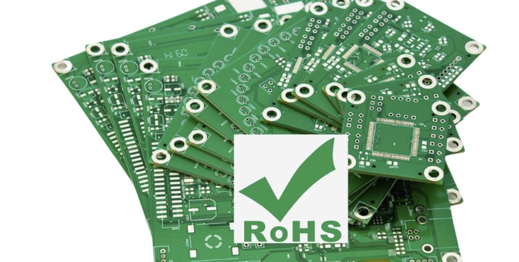
1. RoHS (Restriction of Hazardous Substances Directive)
The European Union’s RoHS directive restricts the use of six hazardous substances in electrical and electronic equipment:
- Lead (Pb)
- Mercury (Hg)
- Cadmium (Cd)
- Hexavalent chromium (Cr6+)
- Polybrominated biphenyls (PBB)
- Polybrominated diphenyl ethers (PBDE)
RoHS compliance is now standard practice in PCB design for products sold in global markets.
2. REACH (Registration, Evaluation, Authorization, and Restriction of Chemicals)
REACH regulations ensure the safe use of chemicals in PCB manufacturing, requiring the registration and risk assessment of substances used in the EU.
3. WEEE (Waste Electrical and Electronic Equipment Directive)
The WEEE directive promotes the recycling and recovery of electronic waste, reducing the environmental impact of discarded PCBs.
4. China RoHS and US Regulations
Other regions, including China and the US, have enacted similar restrictions on hazardous substances in PCB fabrication.
Safe PCB Design and Green PCB Manufacturing Practices
The PCB manufacturing industry is transitioning toward safer practices that minimize environmental and health impacts while maintaining performance and reliability.
1. Lead-Free Soldering
Replacing traditional lead-based solder with lead-free alternatives (e.g., SnAgCu alloys) reduces health risks and ensures compliance with RoHS regulations.
2. Halogen-Free Laminates
Developers now use halogen-free laminates that do not contain brominated flame retardants. These materials lower toxic gas emissions during fires and reduce the environmental impact of discarded boards.
3. Eco-Friendly Surface Finishes
Surface finishes like ENIG (Electroless Nickel Immersion Gold), OSP (Organic Solderability Preservative), and Immersion Silver provide reliable solderability and corrosion protection without relying on hazardous chemicals.
4. Closed-Loop Wastewater Systems
Modern PCB fabrication facilities implement closed-loop systems that treat and recycle wastewater, preventing contamination of water supplies.
5. Safer Etching and Plating Solutions
Alternatives to hazardous etchants like ferric chloride are now available, including alkaline etching solutions that are less harmful and easier to recycle.
6. Recycling and E-Waste Management
PCB manufacturing companies are investing in recycling programs to recover valuable metals (gold, silver, copper) from old PCBs while minimizing environmental damage from improper disposal.
How PCB Hazardous Material Impacts the Lifecycle of Electronic Products
The consideration of PCB hazardous material extends beyond PCB design and PCB manufacturing to the entire lifecycle of the product:
- Manufacturing: Safe material selection reduces health risks for factory workers.
- Usage: Halogen-free materials lower the risk of toxic gas emissions in case of fire.
- Disposal: Environmentally friendly materials facilitate easier recycling and reduce pollution from e-waste.
By designing for environmental compliance from the outset, PCB design teams can minimize product recalls, avoid legal complications, and enhance brand reputation.
Arshon Technology’s Commitment to Safer PCB Design and Manufacturing
At Arshon Technology, we recognize the importance of reducing hazardous materials in PCB fabrication and PCB manufacturing. Our experienced team follows industry best practices and adheres to RoHS, REACH, and other global regulations to deliver eco-friendly and safe PCB design solutions.
Whether you’re developing consumer electronics, automotive systems, or industrial controls, Arshon ensures your PCBs meet environmental standards without compromising performance. Our green manufacturing initiatives include:
- Sourcing lead-free and halogen-free materials.
- Utilizing low-impact surface finishes.
- Partnering with responsible recycling providers for end-of-life PCB management.
Arshon Technology’s commitment extends beyond compliance; we aim to lead by example in promoting sustainability and reducing the environmental impact of electronic products.
Conclusion
PCB hazardous material remains a critical consideration for everyone involved in PCB design, PCB fabrication, and PCB manufacturing. As environmental regulations tighten and consumer awareness increases, companies must prioritize safer materials, responsible manufacturing practices, and effective recycling programs.
By understanding the hazards associated with common substances in PCBs and adopting eco-friendly alternatives, the electronics industry can reduce its environmental footprint while protecting human health.Partnering with experienced providers like Arshon Technology ensures your PCB projects are not only compliant but also aligned with modern sustainability goals.