
Artificial intelligence (AI) is no longer confined to cloud data centers and research labs—it now powers autonomous vehicles, medical‑diagnostic equipment, industrial robots, and even everyday consumer devices. To deliver the compute density, energy efficiency, and real‑time responsiveness that modern AI workloads demand, engineers rely on purpose‑built hardware platforms that push the limits of PCB design and PCB manufacturing.
This in‑depth guide (≈ 2 300 words) dissects the critical design domains that turn silicon brilliance into deployable AI systems. Whether you are crafting a GPU carrier board, an edge‑AI module, or a rack‑scale inference accelerator, the principles below will help you achieve first‑pass success and long‑term reliability.
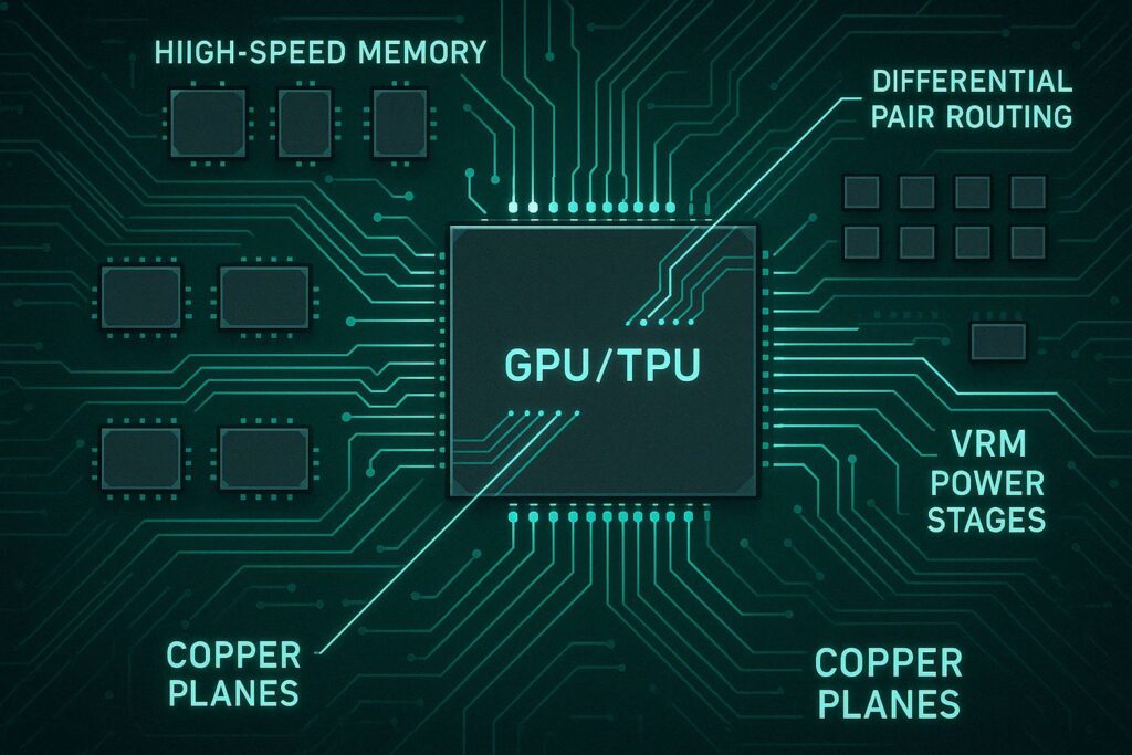
AI Hardware
AI hardware encompasses any electronic subsystem optimized for machine‑learning tasks. The category includes:
| Technology | Typical Role in AI | Key PCB Implications |
| GPUs (e.g., NVIDIA Hopper) | Parallel floating‑point crunching for training & inference | 16–32 Gbps differential pairs, massive VRM current, dense BGA escape routing |
| TPUs/NPUs | Matrix/tensor math acceleration in data centers or edge | Tight power‑integrity budgets (<5 mV ripple), exotic substrates for 112 Gbps SerDes |
| FPGAs | Reconfigurable inference & pre‑processing | Multi‑gigabit transceiver routing (GTY/GTH), flexible I/O banks, dynamic partial reconfiguration |
| ASICs | Fixed‑function accelerators for power‑constrained devices | Ultra‑fine pitch, densely stacked die, advanced HDI/flex integration |
| SoCs with AI co‑processors | All‑in‑one compute on mobiles, drones, IoT | RF coexistence, low‑profile packages, mixed‑signal layout practices |
From a PCB design standpoint, these devices impose three overarching challenges:
- Extreme bandwidth: Hundreds of differential lanes running above 28 Gbps with sub‑ps jitter budgets.
- Explosive current transients: Hot AI engines can toggle entire logic banks in a single clock cycle, demanding milliohm‑class power distribution networks (PDNs).
- Thermal density: Junction temperatures easily exceed 120 °C without aggressive heat‑removal strategies.
Understanding these realities guides every subsequent layout decision.
Specific Requirements
Designing PCBs for AI hardware is uniquely multidisciplinary, blending signal‑integrity science, power‑electronics savvy, and mechanical‑thermal co‑design. Below are the non‑negotiable requirements you must bake into your board specification.
1. High‑Speed Signal Integrity
- Impedance control: Maintain ±5 % tolerance for 50 Ω single‑ended and 100 Ω differential pairs.
- Length matching: For GDDR6 memory buses or PCIe 5.0 links, skew budgets can be as tight as 5 mil (0.127 mm) trace‑length difference between pairs.
- Crosstalk mitigation: Use broadside Coupled microstrip or stripline with solid reference planes. Employ guard traces or stitching vias between aggressor‑victim lanes.
- Return‑path continuity: Strategically place stitching capacitors where layer transitions occur to ensure low‑inductance signal return.
2. Robust Power Distribution Networks (PDNs)
- Low impedance: Aim for < 5 mΩ up to the highest AI clock harmonic (often >300 MHz).
- Bulk & high‑frequency decoupling: Combine tantalum/polymer capacitors with 0402/0201 MLCC arrays located <2 mm from the device pads.
- Power‑train layout: Short, wide copper pours or embedded power planes connect multiphase VRMs to AI silicon; avoid 90° corners to reduce inductance.
3. EMI / EMC Compliance
AI boards radiate significant broadband noise. Enforce proper shielding (cans, copper pour fences) and adhere to EN 55032 / FCC Part 15 limits.
4. Reliability & Lifecycle
Many AI deployments (e.g., self‑driving taxis) require 10‑year field life. Select components with long product‑change notices (PCNs) and design for field‑rework accessibility.
Material Selection
Choosing the correct laminate stack‑up is foundational to meeting the high‑frequency and thermal targets of AI platforms.
| Material Family | ε_r @ 10 GHz | Loss Tangent (tan δ) | Thermal Conductivity (W/m·K) | When to Use |
| Standard FR‑4 (Tg 135 °C) | 4.3 | 0.020–0.025 | 0.3 | Low‑cost evaluation boards <5 Gbps |
| High‑Tg FR‑4 | 4.1 | 0.016–0.020 | 0.4 | Edge AI <10 Gbps, moderate heat |
| Low‑Loss Hydrocarbon/Ceramic (e.g., Rogers 4350B) | 3.5 | 0.0037 | 0.6 | 10–28 Gbps SERDES, sub‑6 GHz RF coexistence |
| Megtron 6 / Isola I‑Speed | 3.2–3.8 | 0.0020–0.0040 | 0.5 | PCIe 5.0/6.0, 56+ Gbps Ethernet |
| Metal Core (Al/Cu) | ≈4.0 | 0.02 | 1.0–4.0 | LED AI vision arrays, fanless edge modules |
| Ceramic HTCC / LTCC | 7–9 (anisotropic) | 0.0005 | 2–4 | Military/space AI SoP, extreme temp cycles |
Tip: For mixed‑signal AI PCBs merging mmWave radar and digital AI logic, dual‑dielectric stack‑ups (e.g., Rogers‑FR‑4 hybrid) provide RF performance without sky‑high cost.
Laminate choice also impacts PCB manufacturing. Ultra‑low loss materials often require plasma de‑smearing and modified press cycles—engage your fabricator early.
Parallel Processing
AI thrives on data‑parallel architectures. Translating that into board‑level performance involves thoughtful layout tactics:
Memory Topology
- GDDR6X/ GDDR7: Route fly‑by topology for command/address (CA) nets and point‑to‑point for data (DQ). Use equal‑length interconnects to all memory devices.
- HBM3 (High‑Bandwidth Memory): Consider silicon interposers or embedded bridge substrates; conventional PCBs struggle with the sub‑200 µm microbump pitches.
High‑Density Interconnect (HDI)
- Microvias & any‑layer builds enable short, obstacle‑free paths between stacked BGAs.
- Sequential lamination allows blind/buried via structures, minimizing layer usage while preserving signal integrity.
Synchronization Signals
Clock and reset nets must be length‑matched and isolated from switching power planes to prevent jitter coupling.
Routing Automation vs. Hand‑Tuning
AI boards often exceed 10 000 nets. Use constraint‑driven autorouting for the bulk, then hand‑tune critical differential lanes and power‑planes to meet target impedance.
Thermal Management
Failing to control heat is the fastest route to degraded inference accuracy and field returns. Combine these strategies:
1. Board‑Level Techniques
- Thermal Vias: Arrays under heat‑spreading copper pours wick heat to inner copper planes or an attached heat sink.
- Copper Coin Inserts: Thick copper slugs embedded in the board channel heat directly away from hot dies.
- Heavy Copper (>3 oz) Layers: Increase current‑carrying capacity in VRM stages and distribute heat.
2. Mechanical Cooling Aids
- Vapor Chambers & Heat Pipes: Efficiently spread heat across heat sinks in 1U/2U server chassis.
- Cold Plates with Liquid Coolant: Essential for >700 W accelerator cards where convective air cooling maxes out.
- Phase‑Change Materials (PCMs): Gel pads absorb thermal spikes for edge devices with bursty workloads.
3. Simulation & Validation
Run CFD simulations (Ansys Icepak, 6SigmaET) coupled with IR thermography field tests to correlate models with reality.
Case Studies
Case Study 1 – NVIDIA A100 SXM Module
- Challenge: Deliver 1.7 TB/s of memory bandwidth while dissipating 400 W.
- PCB Solution: 14‑layer Megtron 6 stack‑up, back drilled vias for NVLink, heavy copper core under die, vapor‑chamber lid.
- Outcome: Stable 1.53 V GPU rail with <3 mV droop during full‑tensor operations.
Case Study 2 – Google Coral Edge TPU Dev Board
- Challenge: Fit 4 TOPS/W ASIC, Wi‑Fi/BT radios, and 4K camera interface on credit‑card footprint.
- PCB Solution: Six‑layer high‑Tg FR‑4 with Rogers 3003 RF sub‑panel, castellated edges for module reflow, stitched RF/logic ground separation.
- Outcome: Passes FCC, operates fanless at 55 °C ambient.
Case Study 3 – Autonomous‑Vehicle Sensor Fusion Unit
- Challenge: Aggregate lidar, radar, and camera data into an AI‑SoC in <10 ms.
- PCB Solution: 18‑layer any‑layer HDI with stacked microvias, copper coins under SoC, 8‑phase digital VRM, liquid cooling cold plate.
- Outcome: <2.5 ms deterministic latency, survives –40 °C to +105 °C automotive profile.
Case Study 4 – Wearable Health‑AI Patch
- Challenge: Continuous ECG/PPG analysis with edge inference in a 1‑mm‑thick flexible form factor.
- PCB Solution: Polyimide flex with plated‑through vias, silver‑ink antennas, and embedded NTC thermistors for adaptive throttling.
- Outcome: 24‑hour battery life, washable, biocompatible enclosure.
Conclusion
The meteoric rise of artificial intelligence is inseparable from innovations in PCB design and PCB manufacturing. Achieving the performance, power efficiency, and reliability demanded by modern AI workloads hinges on:
- Selecting low‑loss, thermally adept materials compatible with high‑volume fabrication.
- Architecting signal and power planes that sustain multi‑tens‑of‑Gbps lanes and sub‑milliohm PDNs.
- Deploying advanced HDI techniques to unlock density while controlling cost.
- Engineering holistic thermal solutions that maintain silicon within safe operating temperatures under continuous stress.
By mastering these domains—and validating designs through simulation, test, and iteration—engineers can confidently bring AI ideas from concept to market with minimal redesign cycles and maximum return on investment.