
Printed Circuit Boards (PCBs) are a crucial component in modern electronic devices, serving as the backbone for most electronic circuitry. They facilitate the physical and electrical connections between multiple electronic components, making them an essential part of any electronic assembly. The manufacturing process of PCBs consists of several complex steps, each requiring precision and expertise. In this article, we will delve into the intricate PCB manufacturing process, highlighting modern techniques, technologies, and best practices.
Understanding PCB Types
Before discussing the manufacturing process, it’s essential to understand the different types of PCBs available in the market:
1. Single-Sided PCBs
These boards have a single layer of conductive material, mainly used for simpler electronic devices.
2. Double-Sided PCBs
Both sides of the board are used for circuit components. They generally allow for more complex designs.
3. Multi-Layer PCBs
These boards consist of multiple layers of circuitry and are used in high-density applications like smartphones and computers.
4. Flexible PCBs
Made of flexible materials, these PCBs can bend and twist, making them ideal for portable devices.
5. Rigid-Flex PCBs
Combining rigid and flexible PCB technologies, these boards can provide space-saving solutions in complex designs.
6. High-Frequency PCBs
Designed for RF applications, these boards are made from specialized materials to handle high-frequency signals effectively.
Understanding these types helps provide insight into why the manufacturing process may differ based on the desired PCB type.
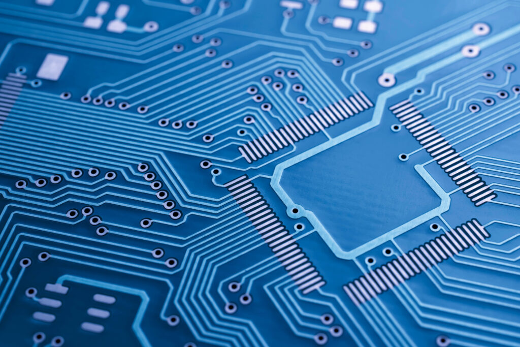
Key Components of a Printed Circuit Board (PCB)
A printed circuit board (PCB) is made up of several key components that facilitate its function in electronic devices. Here are the main parts of a PCB:
1. Substrate
The base material of the PCB, usually made from fiberglass (FR-4) or other dielectric materials. It provides mechanical support and insulation.
2. Copper Layer
A thin layer of copper is applied either on one or both sides of the substrate. The copper forms the electrical pathways (traces) connecting different components.
3. Solder Mask
A protective coating applied over the copper traces to prevent oxidation and solder bridging. It is typically green but can come in other colors.
4. Silkscreen
A layer used for labels, symbols, and markings on the PCB, aiding in component identification and assembly. It’s usually printed in white or yellow.
5. Vias
Small holes that allow electrical connections between different layers of the PCB. They can be through-hole, blind, or buried vias.
6. Traces
Copper lines that connect different components, acting as electrical pathways on the PCB. They can carry signals and power.
7. Pads
Flat areas where components are soldered onto the PCB. They can be used for through-hole or surface-mount components.
8. Components
Various electronic parts soldered onto the PCB, including resistors, capacitors, integrated circuits (ICs), diodes, and connectors.
9. Ground Plane
A large area of copper that serves as a common return path for electric current and helps reduce electrical noise.
10. Power Plane
Similar to ground planes, these are used to distribute power through the PCB efficiently.
11. Edge Connector
A section of the PCB designed to make electrical connections with other circuit boards or components.
12. Mounting Holes
Holes used for securing the PCB to a chassis or enclosure, ensuring it is held in place during operation.
Each of these parts plays a specific role in the overall functionality and performance of the PCB. Understanding these components helps in designing, assembling, and troubleshooting electronic circuits effectively.
PCB manufacturing process flow chart
Creating a flow chart for PCB (Printed Circuit Board) manufacturing involves several key steps.
The steps of the PCB design process start with design and verification and continue through the fabrication of the circuit boards. Many steps require computer guidance and machine-driven tools to ensure accuracy and prevent short circuits or incomplete circuits. The completed boards must undergo strict testing before they are packaged and delivered to customers.
Step 1: Design and Prototyping
In Step 1 of the PCB manufacturing process, we focus on design and prototyping, utilizing PCB design software to create layouts, performing Design Rule Checks (DRC) to ensure compliance with specifications, developing prototypes for testing, and finalizing the design based on feedback and performance evaluations
PCB Design Software
The first step in the PCB manufacturing process is designing the board. Engineers use specialized PCB design software (like Eagle, Altium Designer, or KiCAD) to create the layout. The design includes:
– Schematic Capture: Drawing the circuit using symbols for electronic components.
– Layout: Placing components on the board and routing electrical connections.
Design Rule Checks (DRC):
Once the initial design is created, it undergoes Design Rule Checks (DRC) to ensure that it adheres to manufacturing tolerances, such as minimum trace width and spacing. This step is vital for avoiding faulty designs that may not be manufacturable.
Prototype Development:
After passing DRC, a prototype PCB is often developed. This stage involves:
– Creating a Printout: Using a plotter to create a film or direct-to-film printing of the PCB layout.
– Examining Usability: Checking the layout in a practical scenario to identify potential design flaws.
Finalization of Design:
Once all modifications are made, the final PCB design is prepared, often saved in Gerber format, which is the standard file type used for PCB manufacturing.
Step 2: Material Selection
In Step 2, material selection is critical, where we choose the appropriate base material for the PCB and determine the copper weight to ensure optimal conductivity and performance for the intended application.
Base Material:
The most common base material for PCBs is FR-4, a fiberglass-reinforced epoxy laminate. Depending on the PCB type, other materials may be chosen, such as:
– Polyimide for flexible PCBs.
– PTFE for high-frequency PCBs.
Copper Weight:
The copper weight (measured in ounces) also needs to be determined based on the electrical requirements of the application. Thicker copper layers are used for high-current applications.
Step 3: PCB Fabrication
In Step 3, PCB fabrication involves several key processes, including printing the circuit design onto the substrate, etching the PCB to remove unwanted copper, drilling holes for component placement, and applying plating and surface finishing to enhance conductivity and protect against environmental damage.
Printing the Circuit Design:
The first step in the fabrication process is to transfer the design onto the chosen substrate. This can be achieved through two primary methods:
1. Photo-Plotting
The PCB layout is reproduced onto a light-sensitive material called photoresist. This is often done using a laser printer or plotter.
2. Direct Imaging
A more modern technique where the PCB design is directly imaged onto the substrate without the need for photomasks.
Etching the PCB
Once the design is printed onto the substrate, the next step is etching. In this process, the unwanted copper is removed, leaving behind the desired circuit pattern. This is usually done through various methods:
– Chemical Etching: Involves using a chemical solution (such as ferric chloride) to remove the excess copper.
– Laser Etching: A more advanced technique, using lasers to vaporize the unwanted copper.
Drilling Holes
After etching, holes are drilled into the PCB for component leads. These holes can be small (for surface-mounted components) or large (for through-hole components). Automated drilling machines often perform this task for accuracy.
Plating and Surface Finishing
Following drilling, the PCB is then plated. The plating process involves:
– Through-Hole Plating: Coating the holes with copper to create electrical connections between layers.
– Surface Finishing: Applying a coating (like HASL, ENIG, or OSP) to the surface to prevent oxidation and improve solderability.
Step 4: Layering for multi-layer PCBs
In the case of multi-layer PCBs, additional steps are required to build the layers. This involves:
1. Layer Stacking: Aligning multiple layers of PCB together.
2. Lamination: Using heat and pressure to bond the layers together using epoxy resin.
3. Drilling: New holes are drilled to connect different layers.
Step 5: Quality Assurance
In Step 5, Quality Assurance involves conducting comprehensive visual inspection and X-ray inspection to ensure the highest standards of product integrity and safety.
Quality checks are crucial throughout the PCB manufacturing process. Various tests are conducted to ensure that the PCBs meet industry standards:
Electrical Testing
1. Continuity Testing: Ensures there are no open circuits.
2. Insulation Testing: Checks for short circuits.
Visual Inspection
After fabrication, each PCB undergoes a visual inspection for defects such as burrs or misaligned components.
X-Ray Inspection
For more complex boards, especially those with hidden layers, X-ray inspection can be used to check for internal defects.
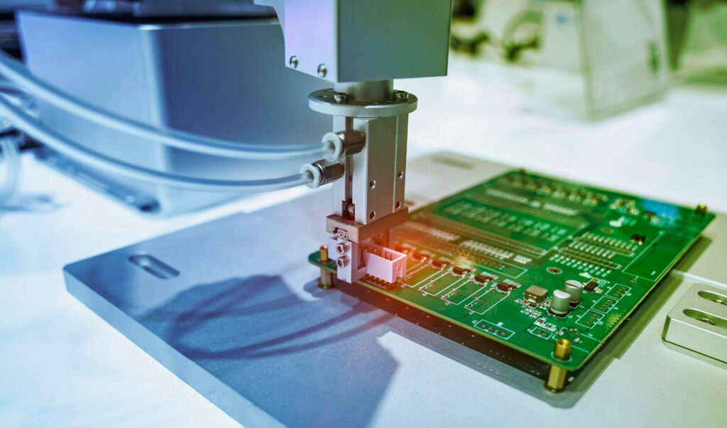
Step 6: Assembly
In Step 6, Once the PCBs are fabricated and pass the quality tests, they are ready for assembly.
The assembly process involves precise component placement on the PCB, followed by careful soldering to ensure secure connections, culminating in a thorough final inspection and rigorous testing to guarantee functionality and reliability.
Component Placement:
1. Surface Mount Technology (SMT): Components are placed on one side of the PCB and soldered.
2. Through-Hole Technology: Components with leads are inserted through holes and soldered on the opposite side.
Soldering
A few common soldering methods include:
– Wave Soldering: A continuous wave of molten solder flows over the board to solder components.
– Reflow Soldering: Used mainly for SMT, where solder paste is applied to pads, components are placed, and the board is heated.
Final Inspection and Testing
After assembly, the PCB undergoes final inspections to ensure all components are correctly soldered and positioned. Automated Optical Inspection (AOI) is frequently used at this stage.
Step 7: Packaging and Shipping
Once the PCB passes all inspections, it is cleaned, packaged, and prepared for shipping. Packaging must ensure that the PCBs do not get damaged during transit.
Equipment Used in PCB Manufacturing
Here are some common types of equipment used in PCB manufacturing:
- Photoplotters: Used for printing high-resolution images of the PCB design onto photo-sensitive film.
- Laser Etching Machines: Used to create detailed patterns on the PCB surface by etching away unwanted copper.
- Drilling Machines: CNC drill machines are used to create holes for component leads and vias.
- Plating Equipment: For the electroplating process, equipment is used to deposit a layer of metal (such as gold or nickel) onto the PCB.
- Solder Mask Application Machines: Used to apply protective coatings that prevent solder from covering unwanted areas of the board.
- Screen Printing Machines: For applying solder paste or silkscreen graphics to the PCB.
- Reflow Ovens: Essential for soldering surface-mounted components by heating the solder paste to its melting point.
- Wave Solder Machines: Used for mounting through-hole components by passing the PCB over a wave of molten solder.
- Testing and Inspection Equipment: Automated Optical Inspection (AOI) machines and X-ray systems ensure quality control by detecting defects.
- Conformal Coating Machines: For applying protective coatings that enhance durability and resistance to environmental factors.
- Pick and Place Machines: Used for accurately placing surface-mount components onto the PCB before soldering.
These tools and machines work together to ensure efficient, accurate, and high-quality PCB manufacturing
Challenges in PCB Manufacturing
The PCB manufacturing process comes with numerous challenges:
– Cost Management: Keeping production costs low without compromising quality.
– Lead Time: Reducing the time taken for prototyping and manufacturing.
– Technology Adaptation: Keeping up with advances in PCB technology.
Emerging Trends in PCB Manufacturing
The PCB industry is experiencing various trends shaping the future of PCB manufacturing:
– Automation: Robotics and AI are beginning to play significant roles in the manufacturing processes, improving efficiency and accuracy.
– Sustainability: There is an increasing emphasis on eco-friendly materials and processes to minimize environmental impact.
– Miniaturization: As electronics become smaller, PCBs must adapt to fit in compact designs.
Arshon Technology’s PCB Design Services
Arshon Technology specializes in delivering comprehensive PCB design services for clients across the USA and Canada.
Arshon expertise encompasses the full PCB design process, beginning with initial concept and schematic development, and continuing through layout and prototype fabrication. The company is dedicated to quality and precision, employing advanced software tools and industry best practices to produce reliable and efficient designs.
Furthermore, Arshon Technology provides customized services tailored to various industries, ensuring that the PCBs fulfill specific client requirements and adhere to regulatory standards. Rigorous quality assurance and thorough testing are essential components of their design process, ensuring that the final products perform reliably in real-world applications.
Conclusion
The PCB manufacturing process is a blend of art and science, requiring meticulous planning, skilled craftsmanship, and advanced technology. As electronics continue to evolve, the demand for high-quality, custom-designed PCBs will grow, necessitating continuous innovation in manufacturing techniques. Understanding this process not only helps manufacturers improve their methodologies but also gives designers insight into what to expect, ensuring the seamless integration of PCBs into the devices of tomorrow.